
Antenna Design Section
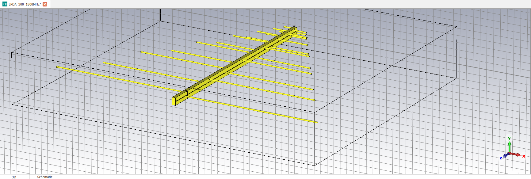
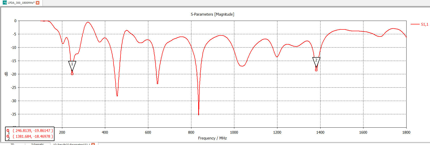
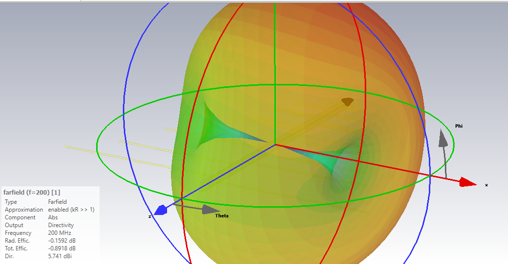
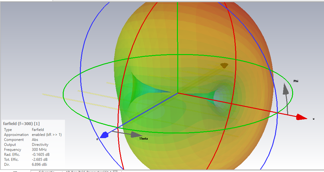
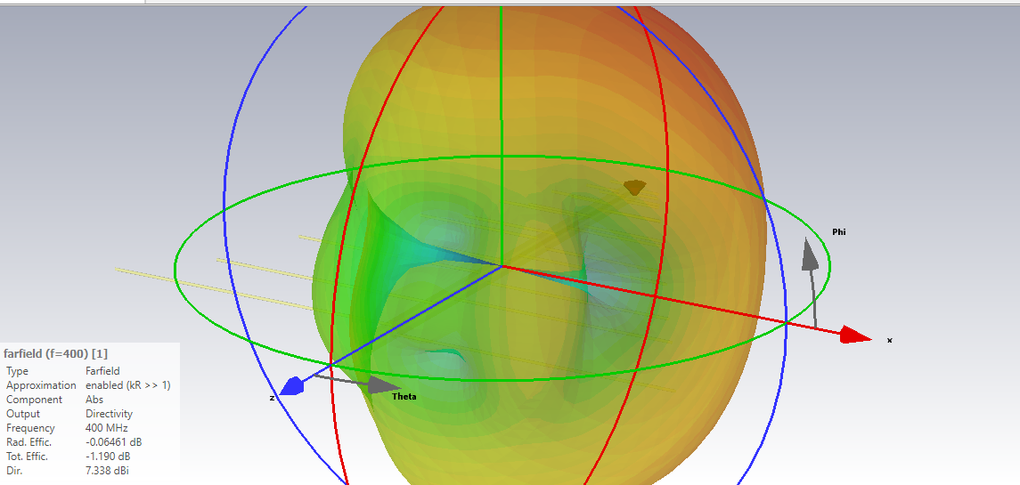
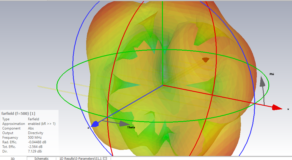
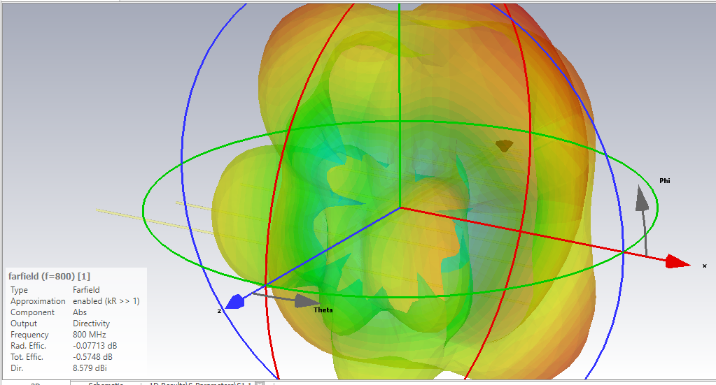
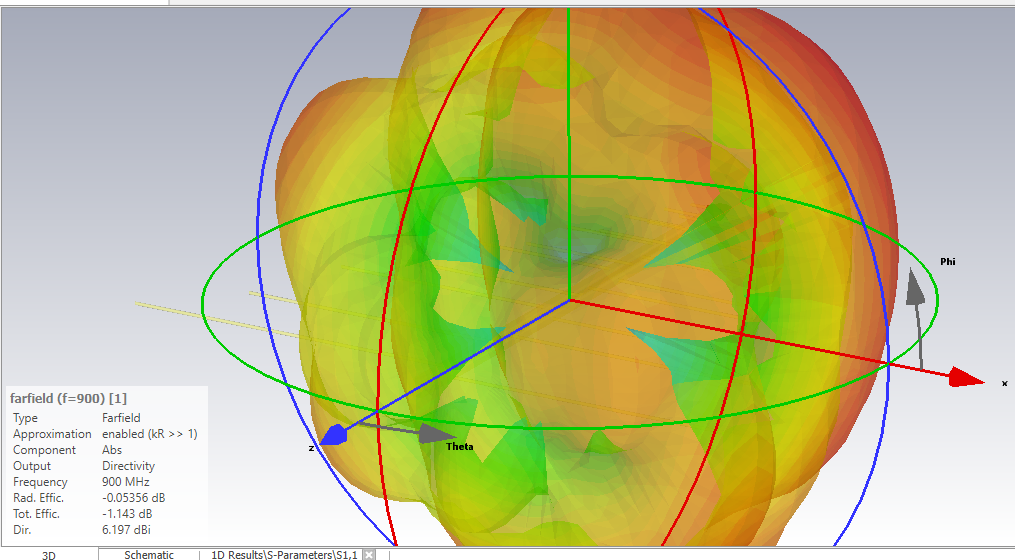
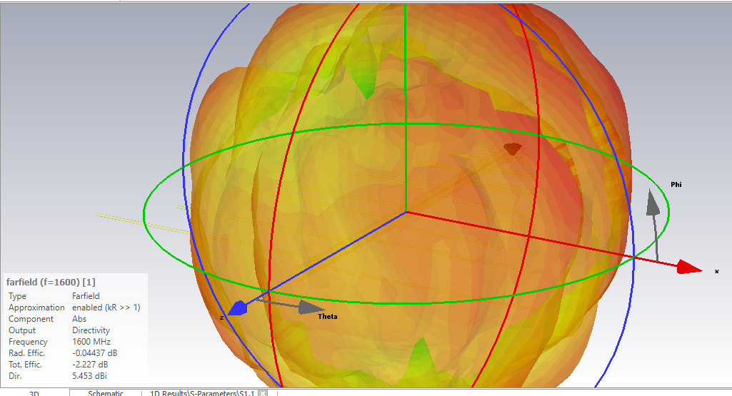
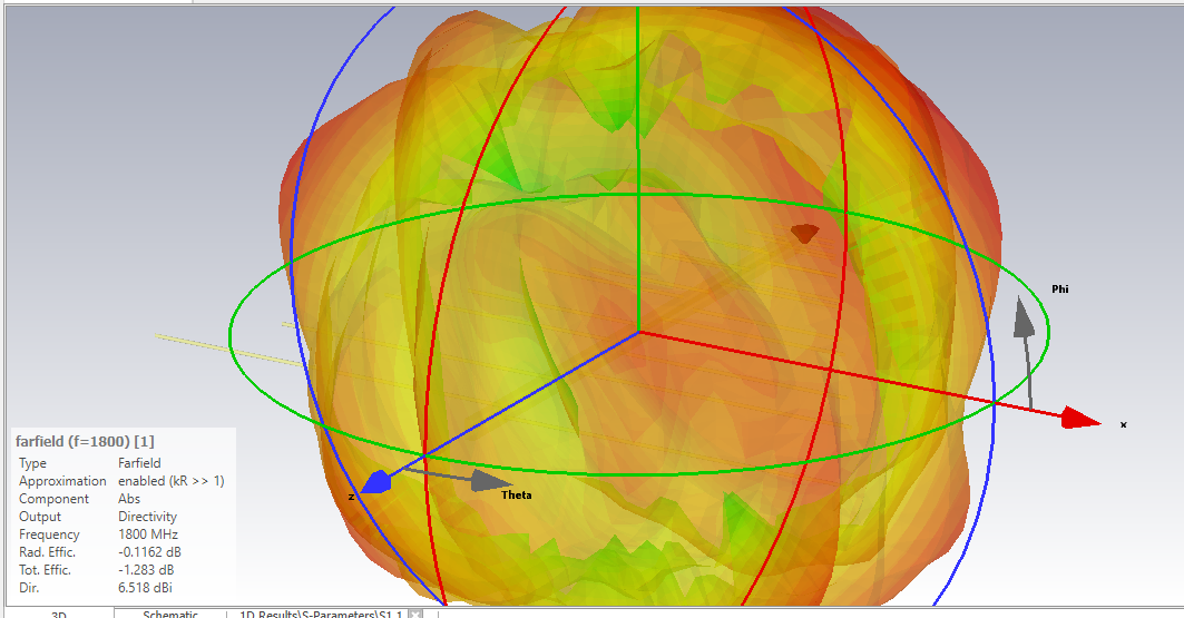
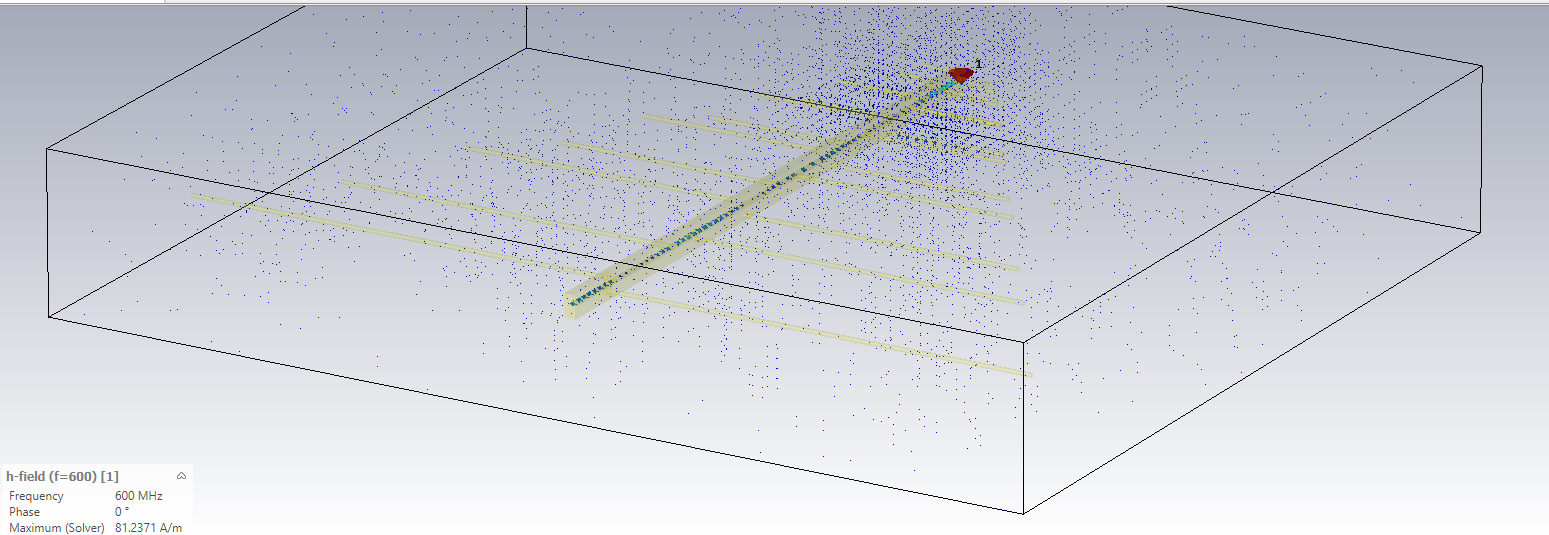
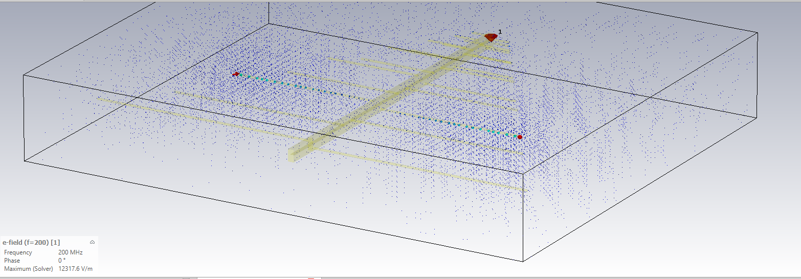
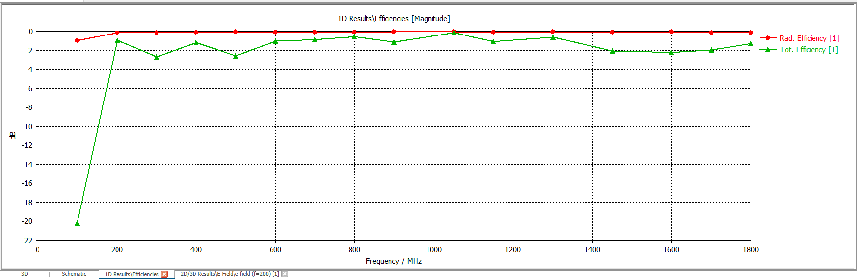
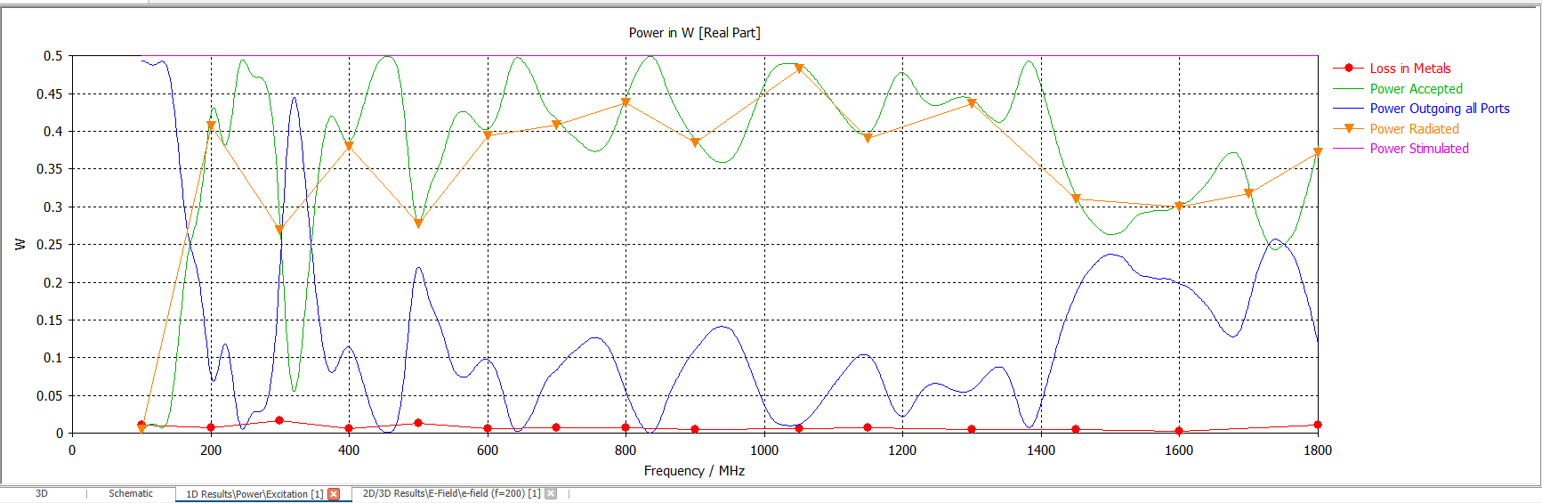
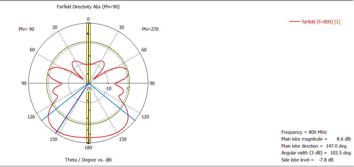
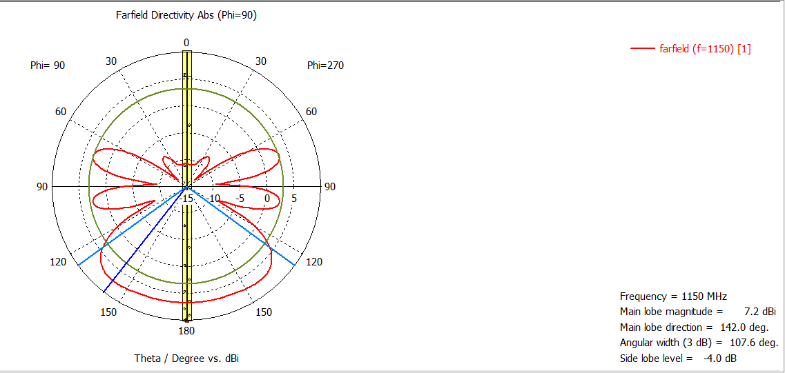
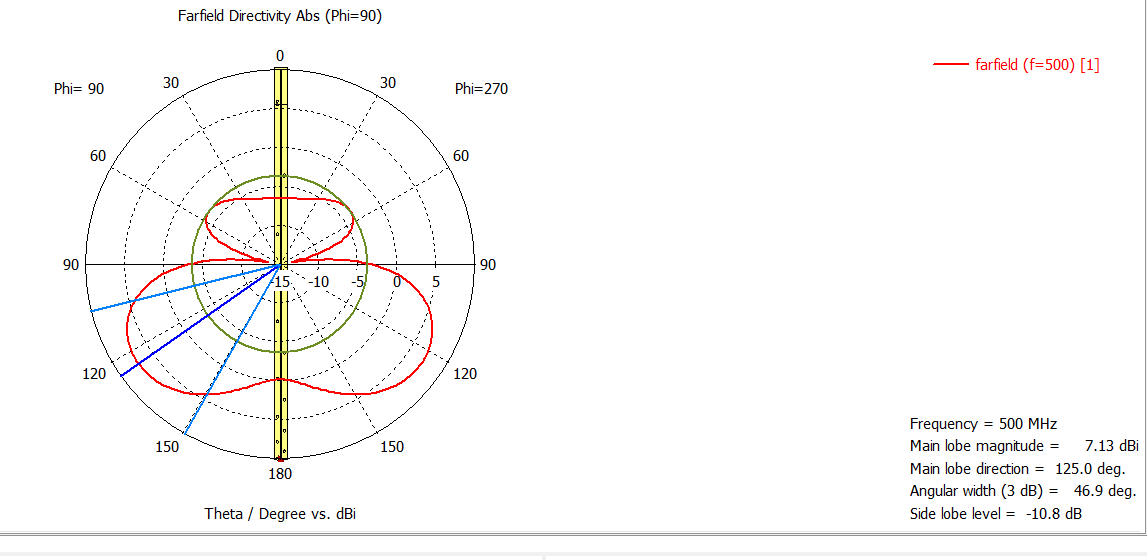
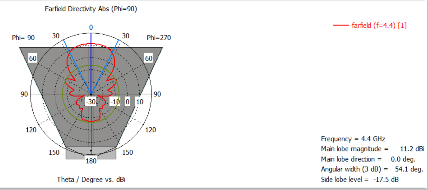
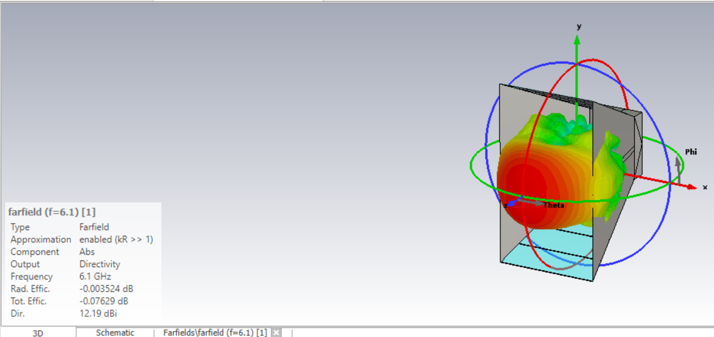
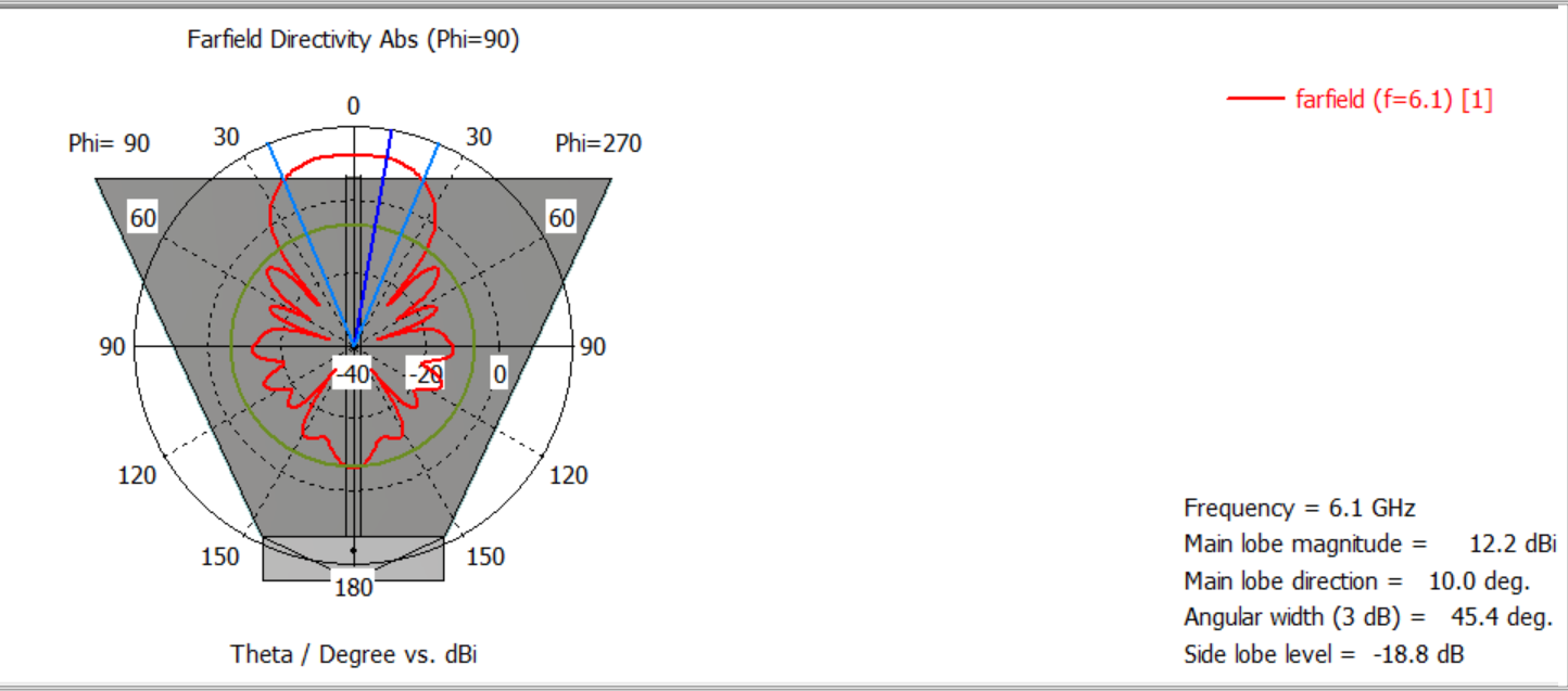
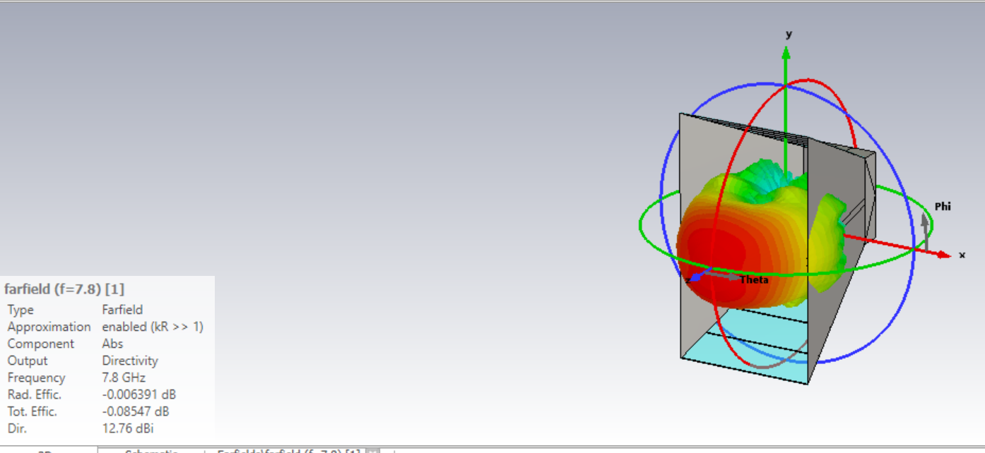
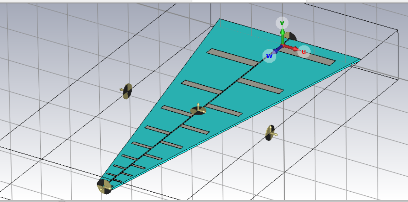
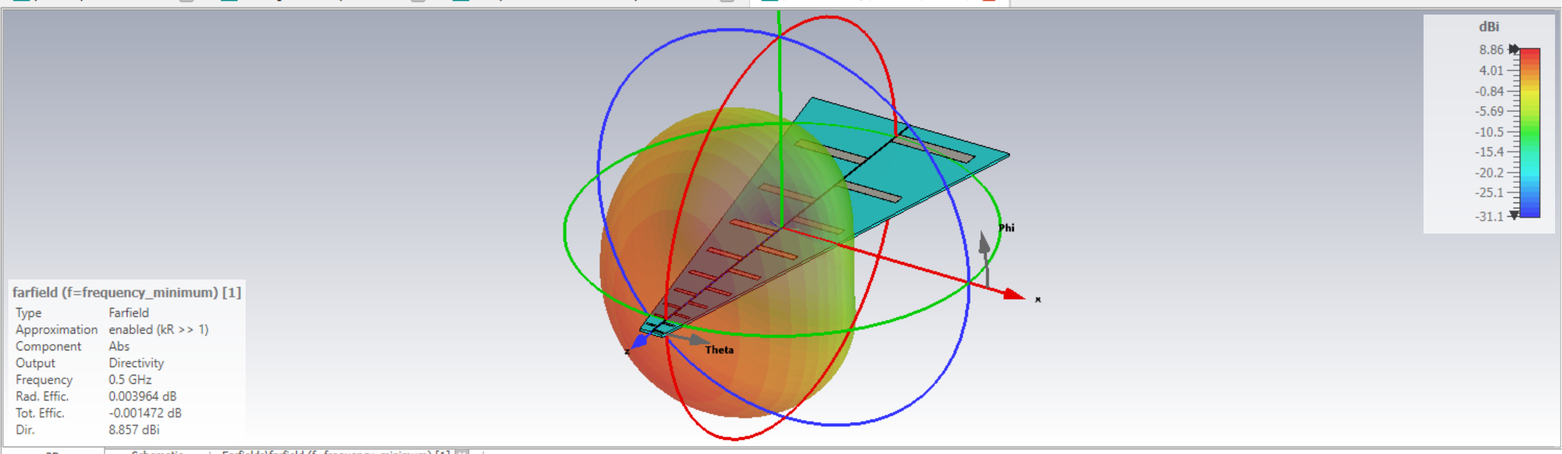
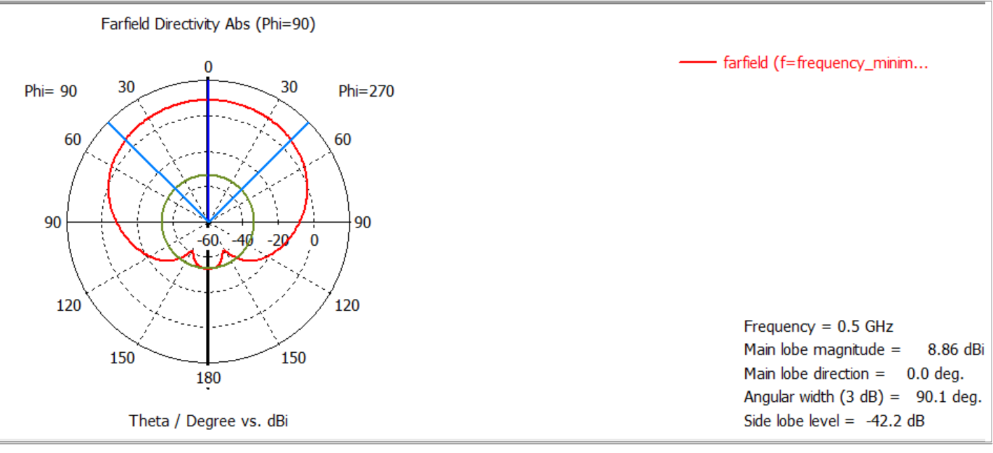
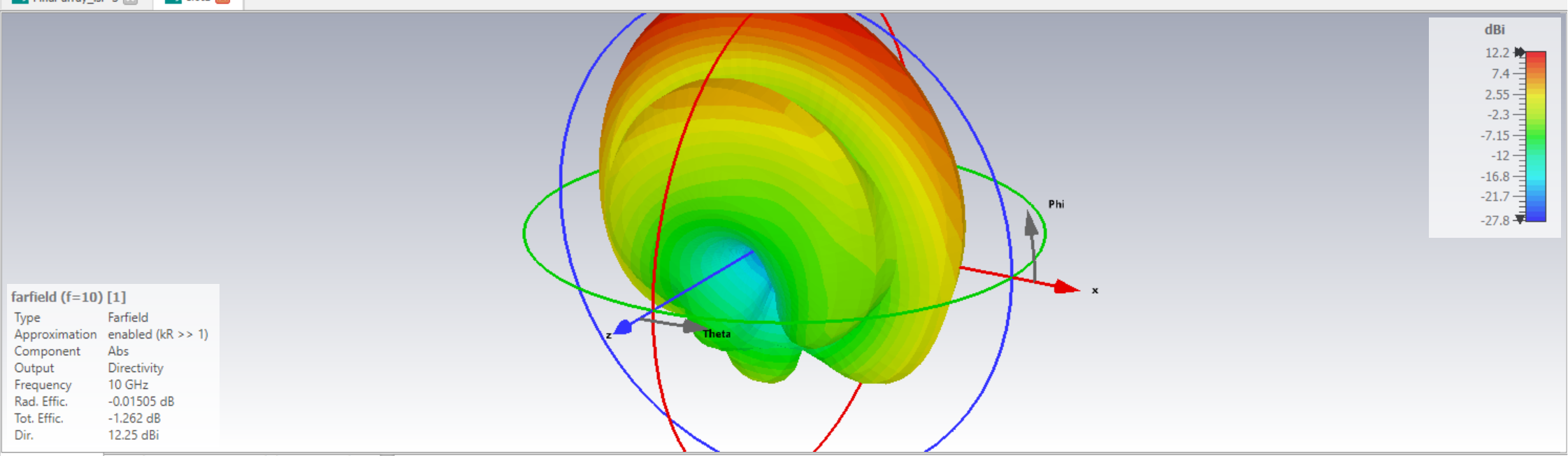
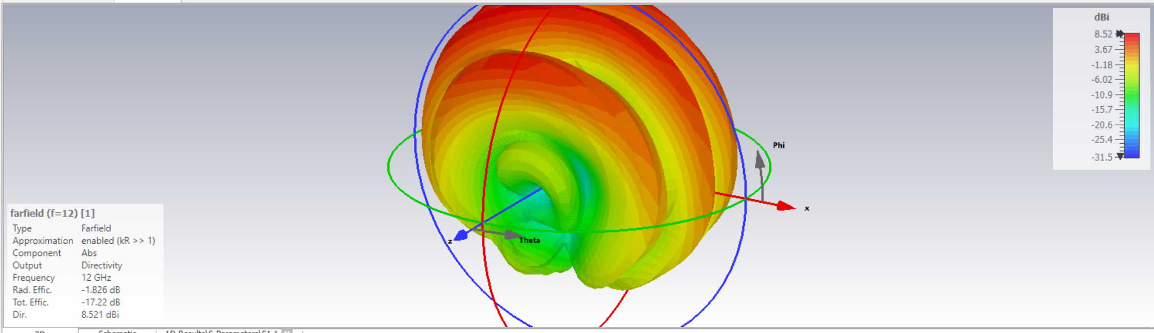
Log-periodic Dipole array from 300 MHz-1300 MHz
Log-Periodic Dipole Array (LPDA) at VHF (300-1300 MHz) – CST Design | Results & Working Principle
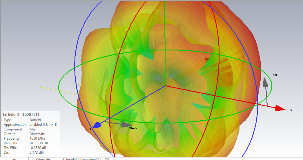
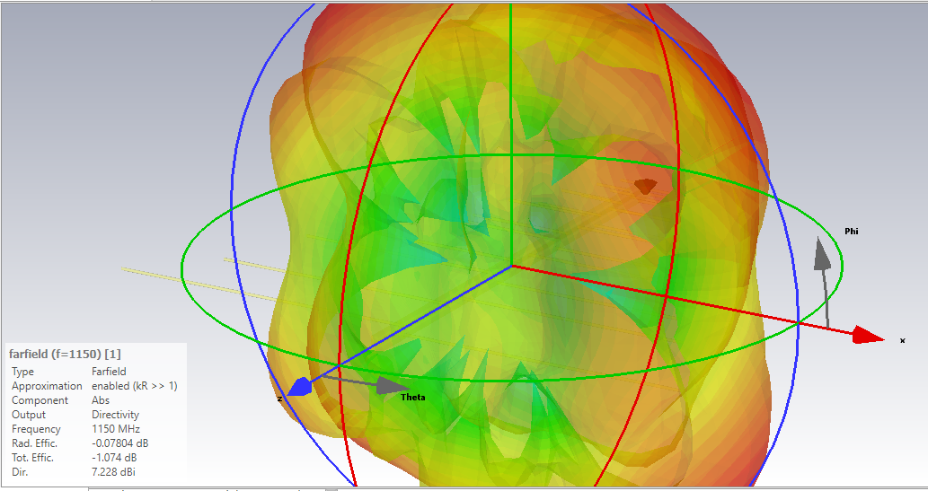
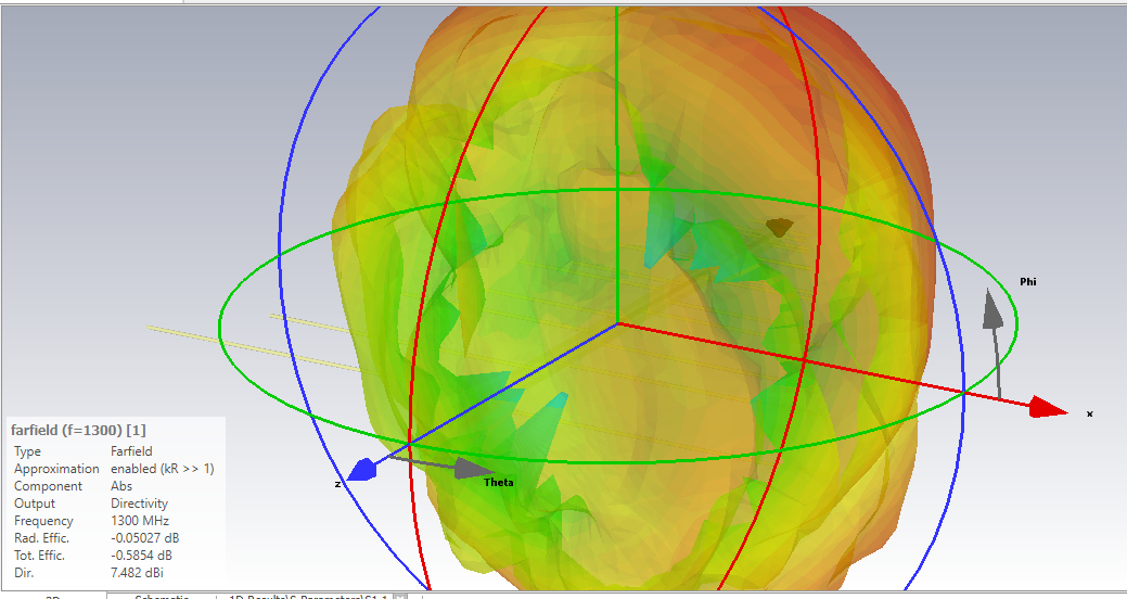
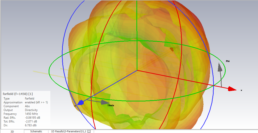
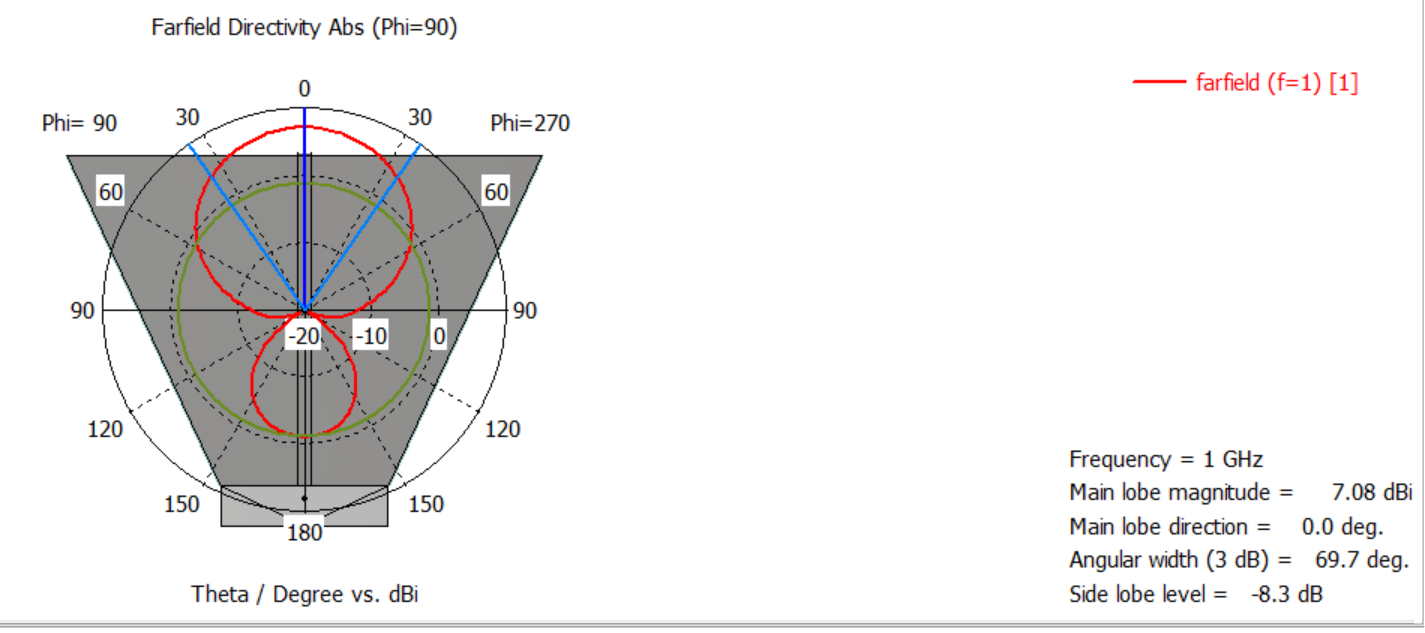
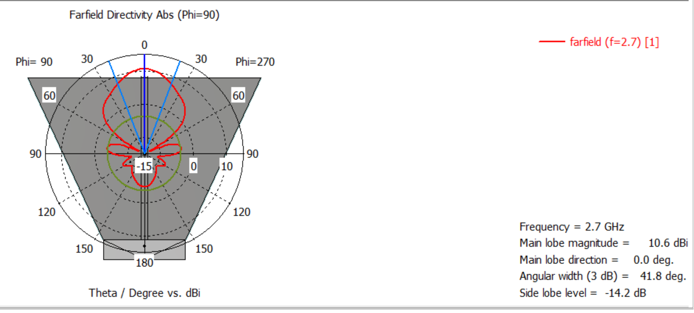
The LPDA consists of multiple dipole elements that progressively decrease in length toward the front, which is the direction of maximum radiation. Adjacent elements are fed with alternating phases, requiring a feed line running along the boom to ensure proper signal phasing.
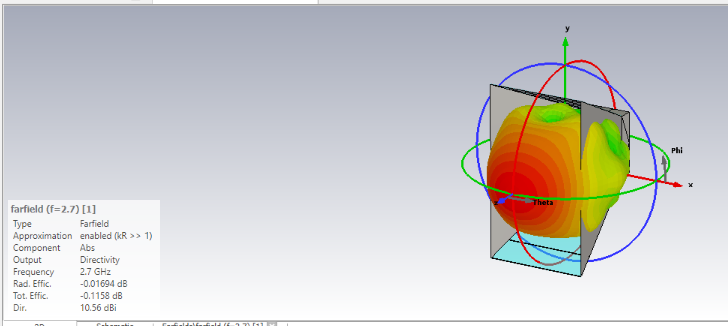
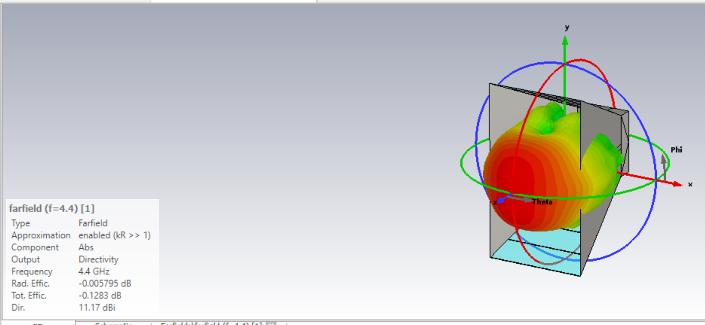
The elements are mounted on a supporting boom and typically made of lightweight conductive materials such as aluminum. Their lengths and spacing follow a logarithmic scaling factor (τ), which defines the array geometry. The longest element corresponds to a half-wavelength at the lowest operating frequency, while the shortest element sets the upper frequency limit. Element spacing also decreases toward the front.
At any given frequency, only a small active region (typically about three elements) effectively radiates, and this active region shifts smoothly along the array as frequency changes. The antenna is usually fed from the shortest element, with the longest element acting as a reflector.
LPDA vs. Yagi–Uda Array
Yagi–Uda antennas provide high, narrowband gain at a specific frequency and are highly directional. In contrast, LPDAs offer moderate gain (≈5–15 dBi) over a wide frequency range with broader radiation patterns and lower directivity. LPDAs typically operate from 30–4200 MHz, while Yagi antennas operate from 30–3000 MHz. Yagi antennas focus energy into a narrow beam, whereas LPDAs provide wider coverage due to varying element lengths and spacing.
Advantages
Wide bandwidth
Directional radiation pattern
Moderate to high gain
Compact size
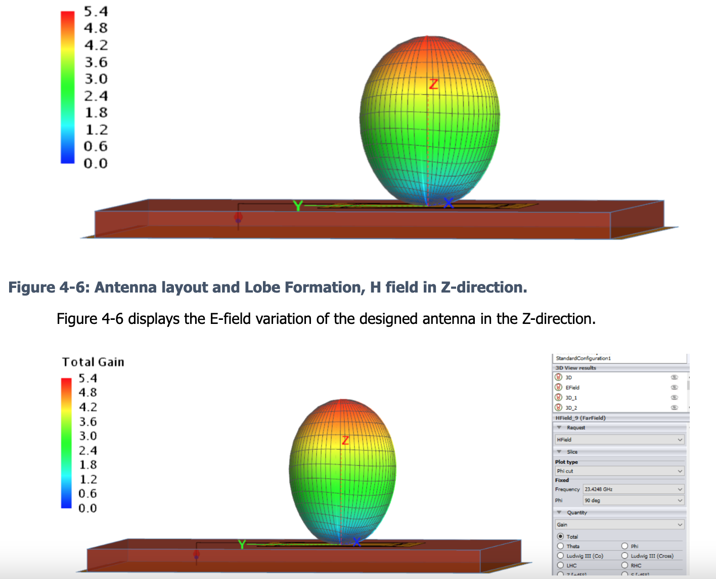
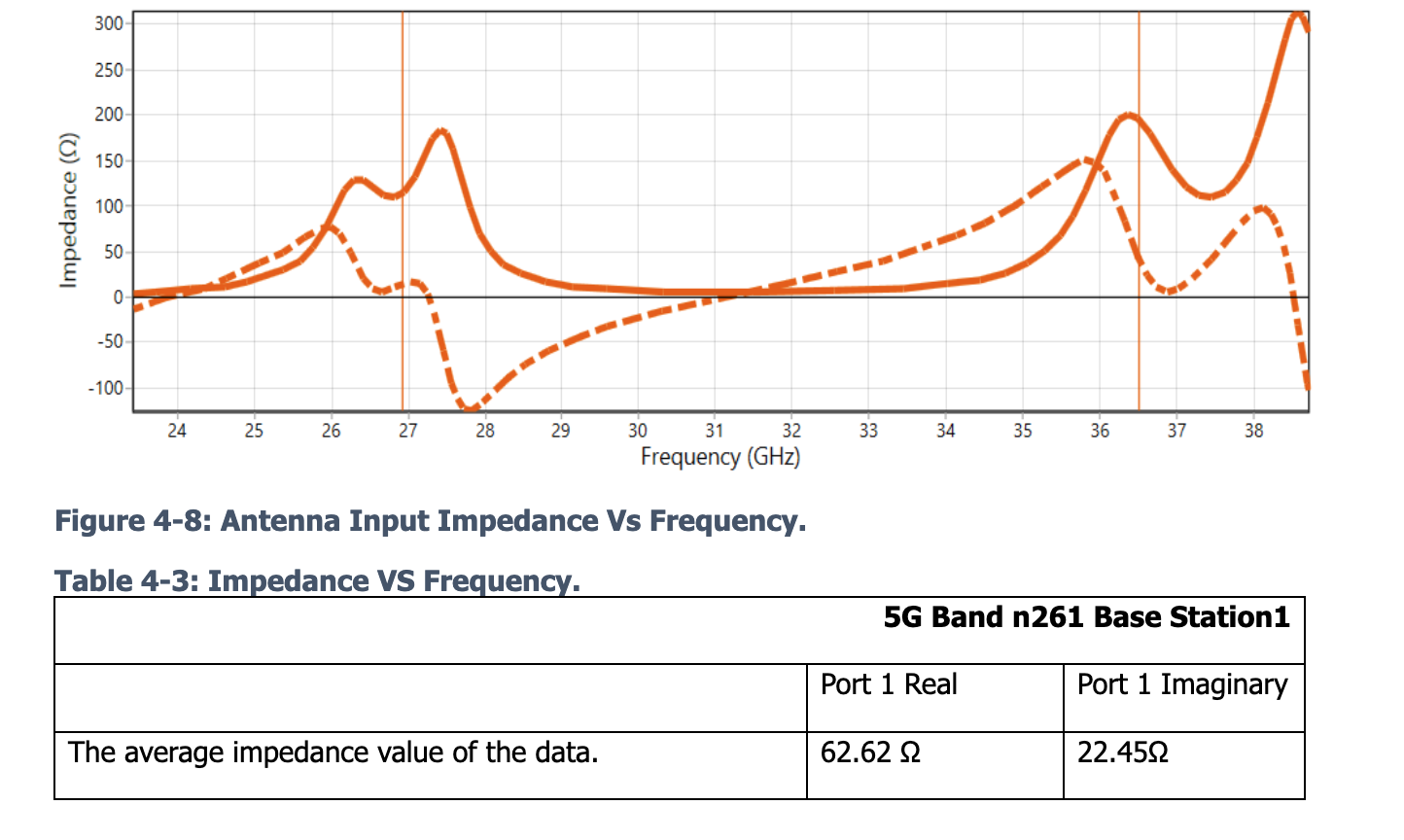
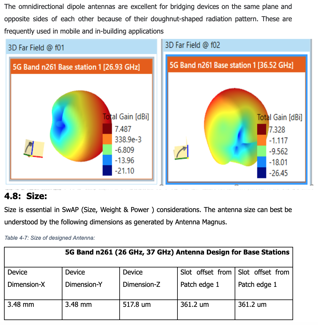
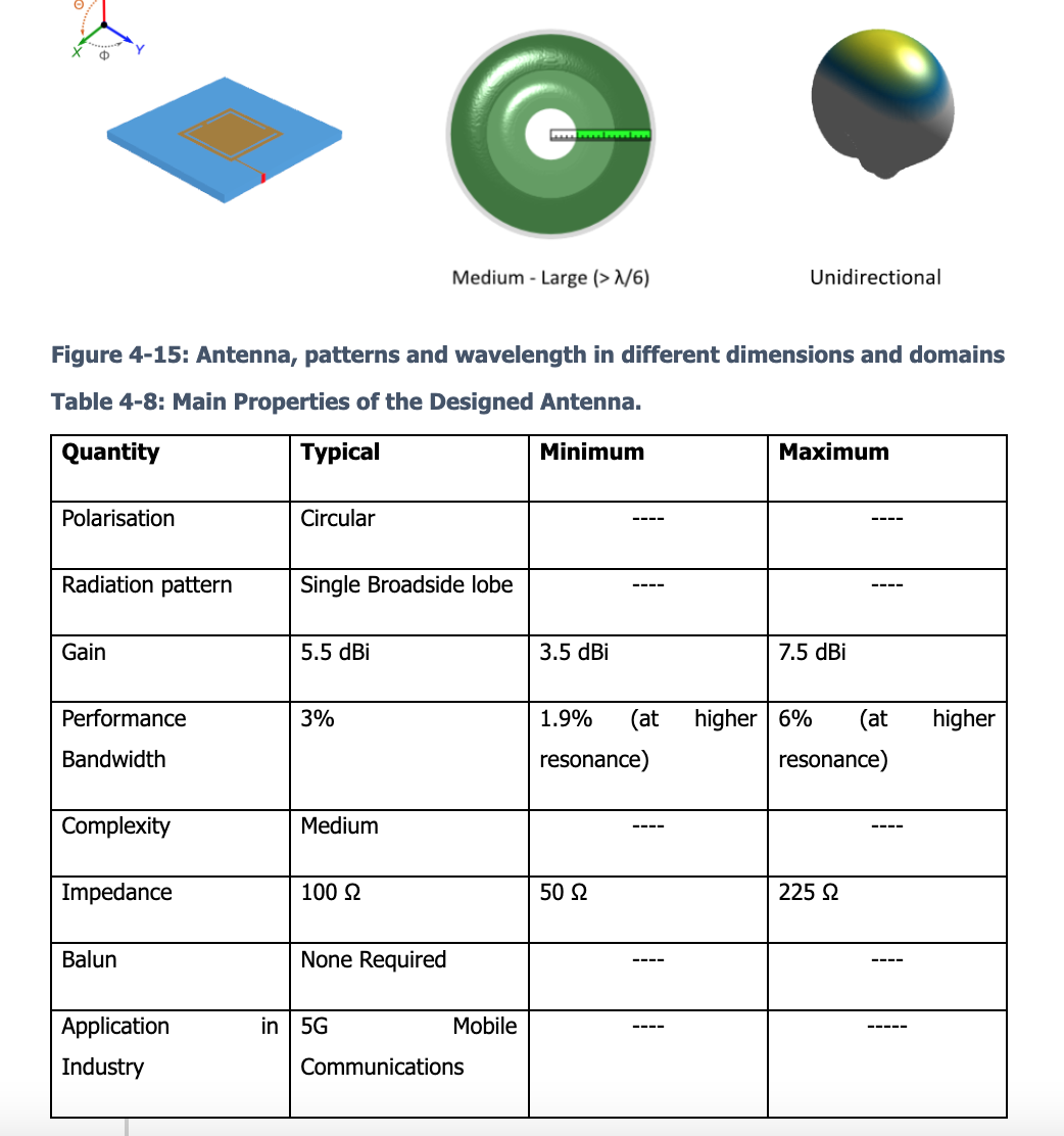
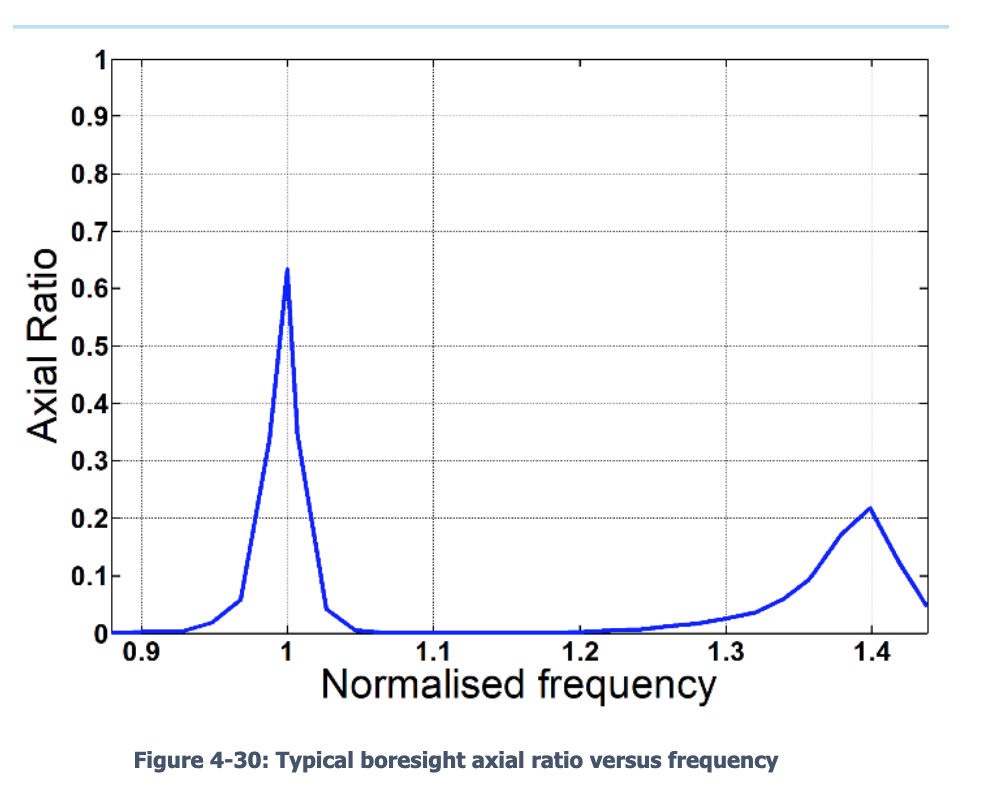
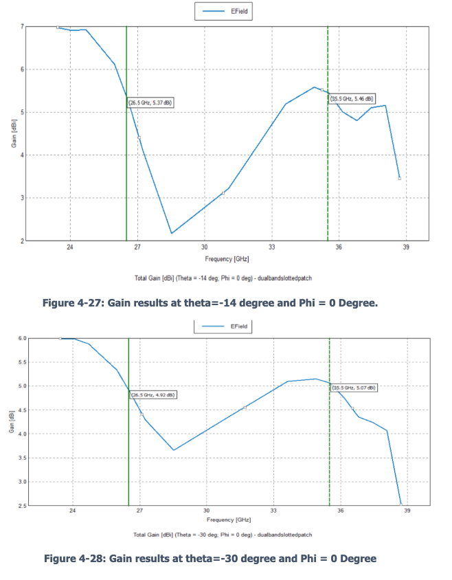
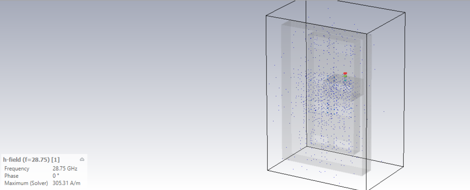
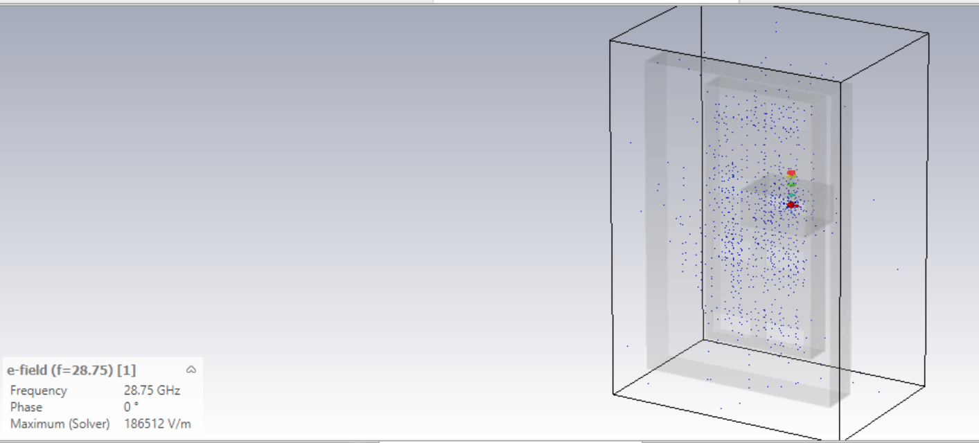
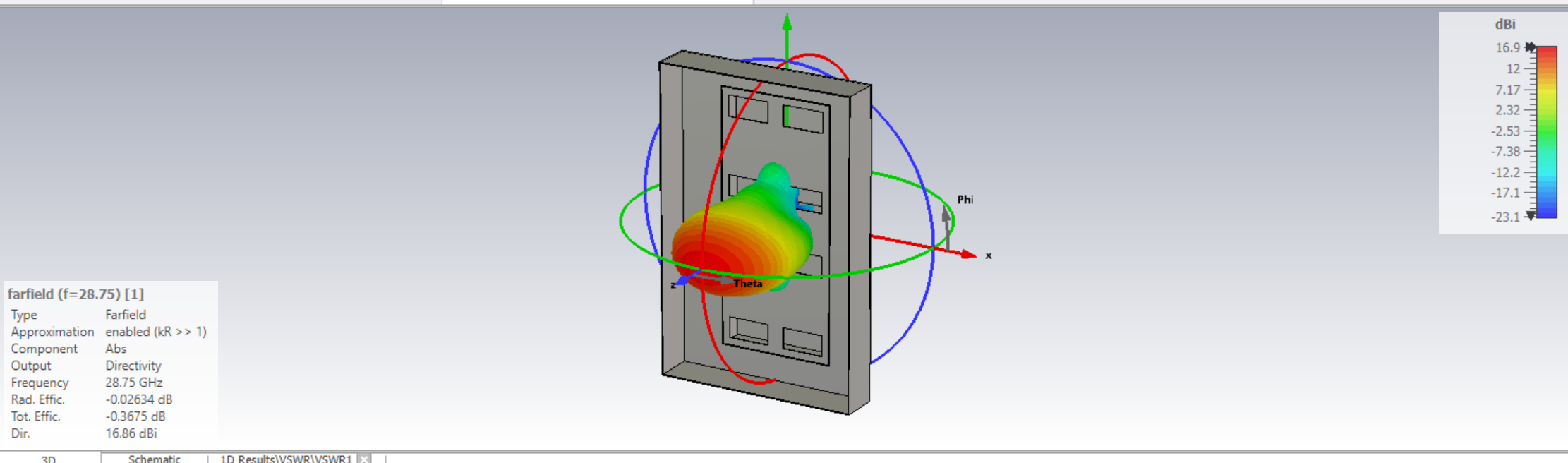
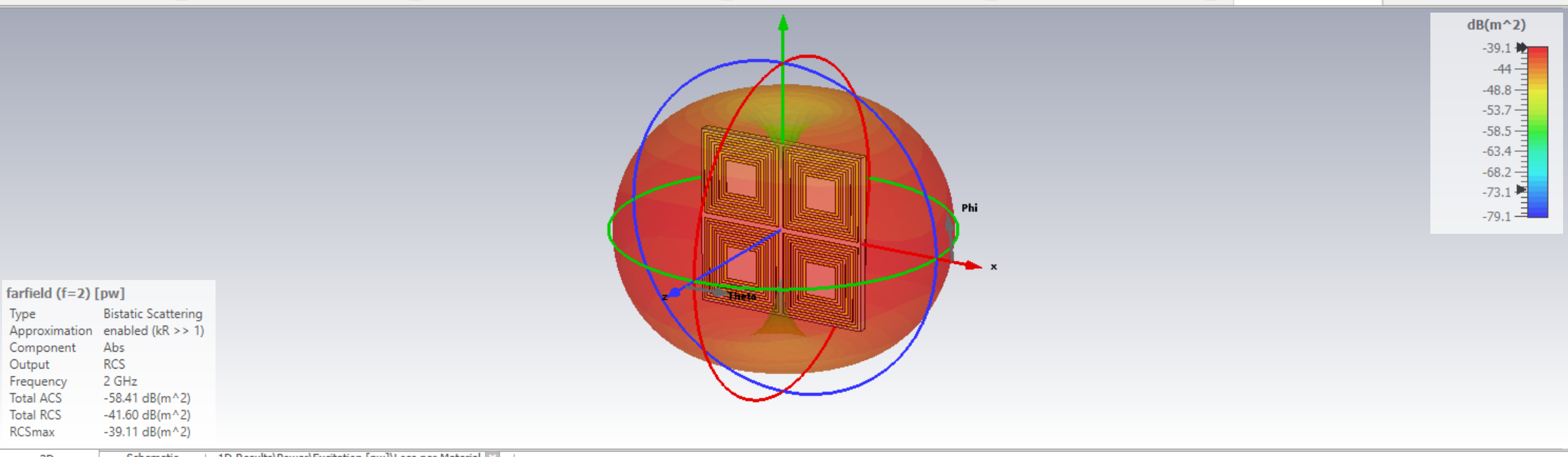
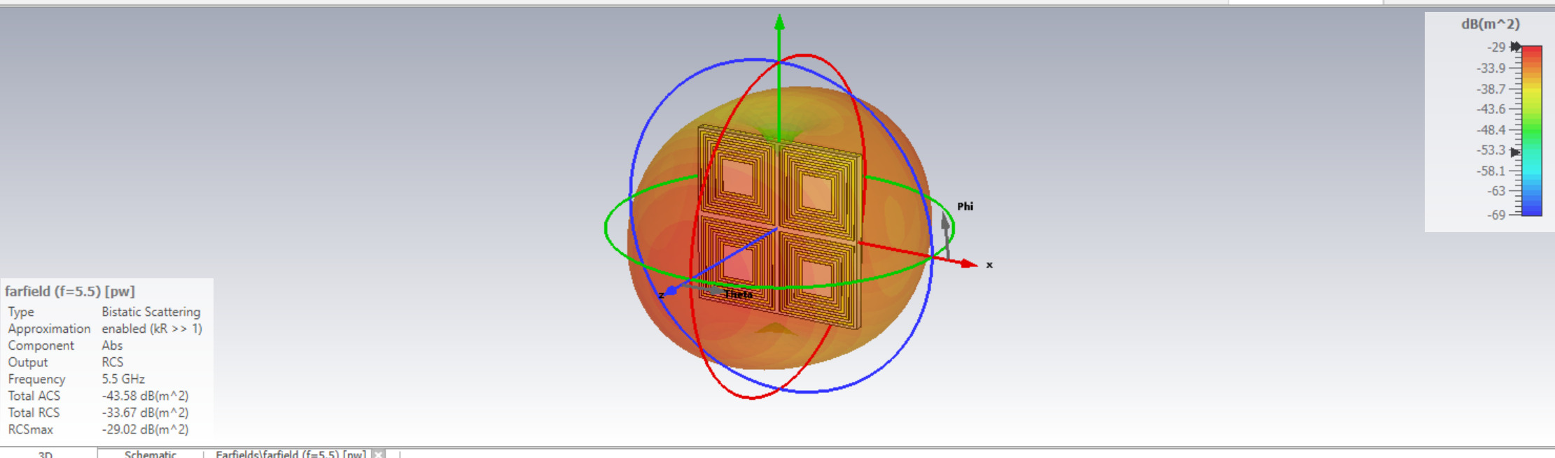
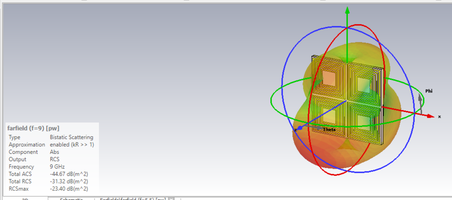
Design of a Multi-band (dualband) Micro-strip slotted Patch Antenna For 5G Wireless Communications
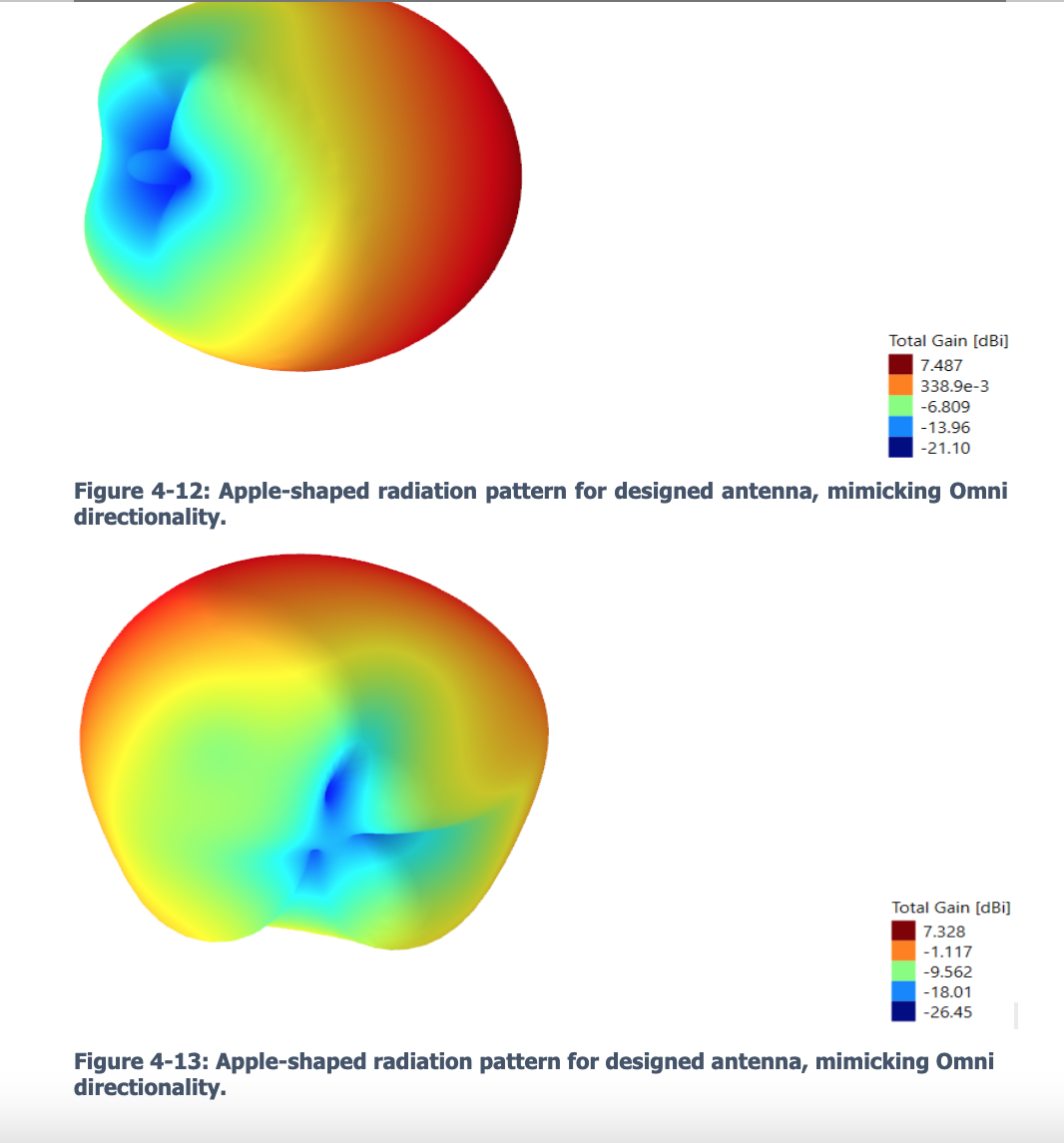
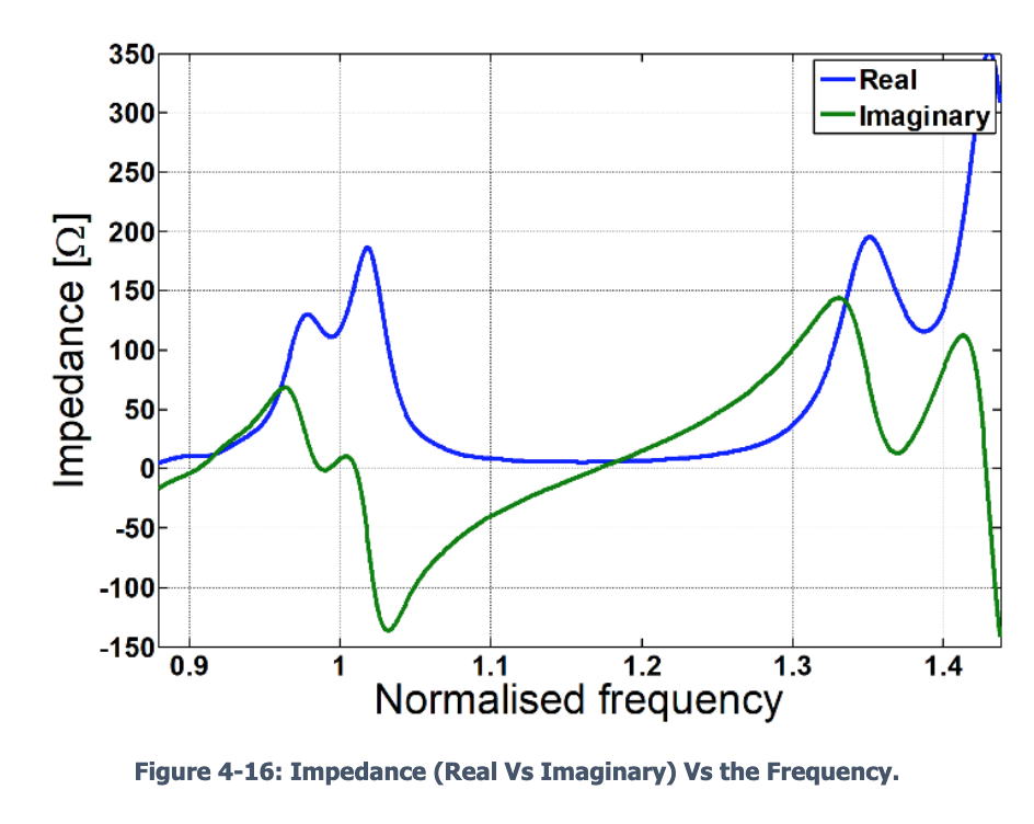
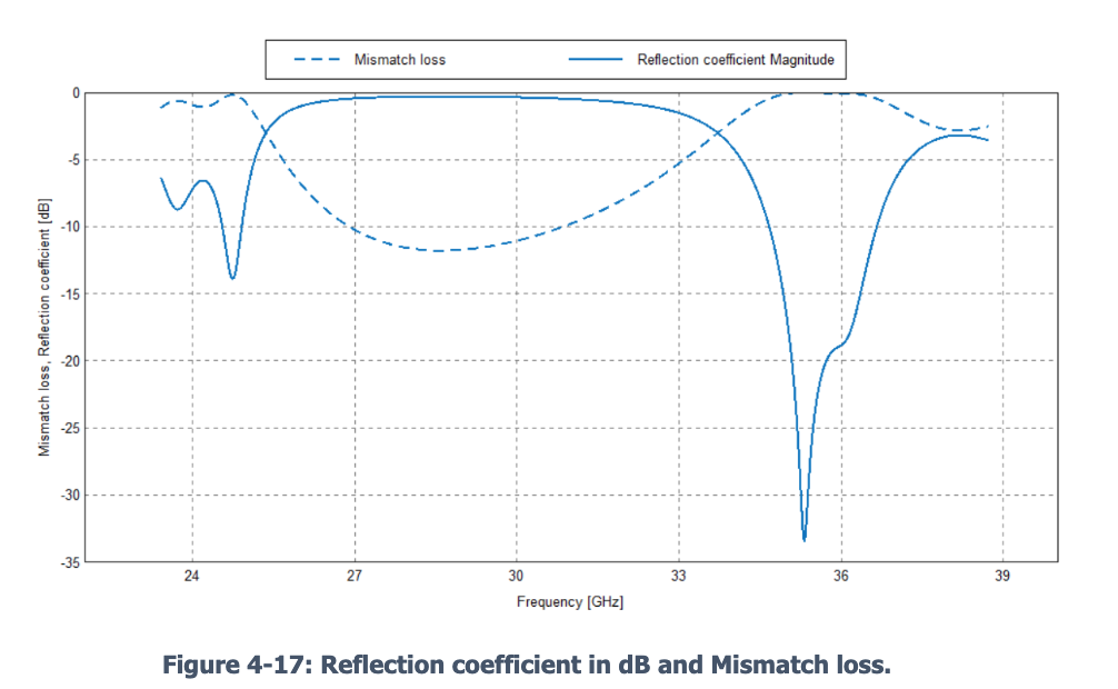
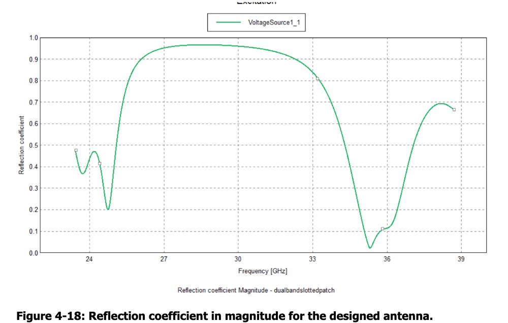
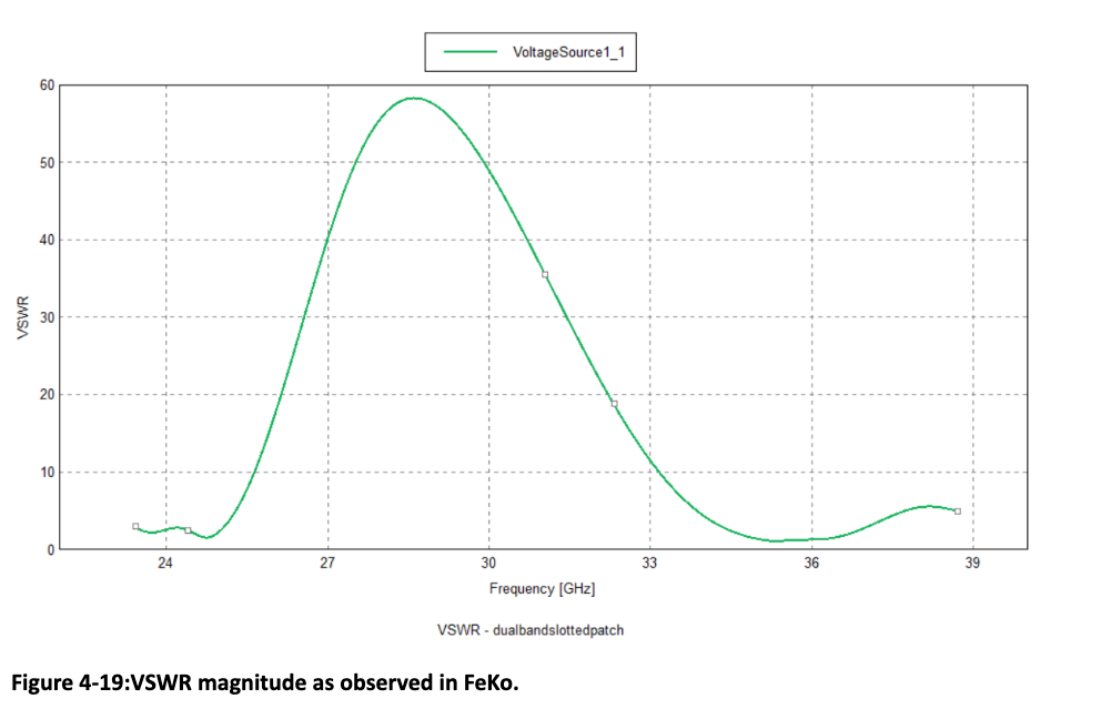
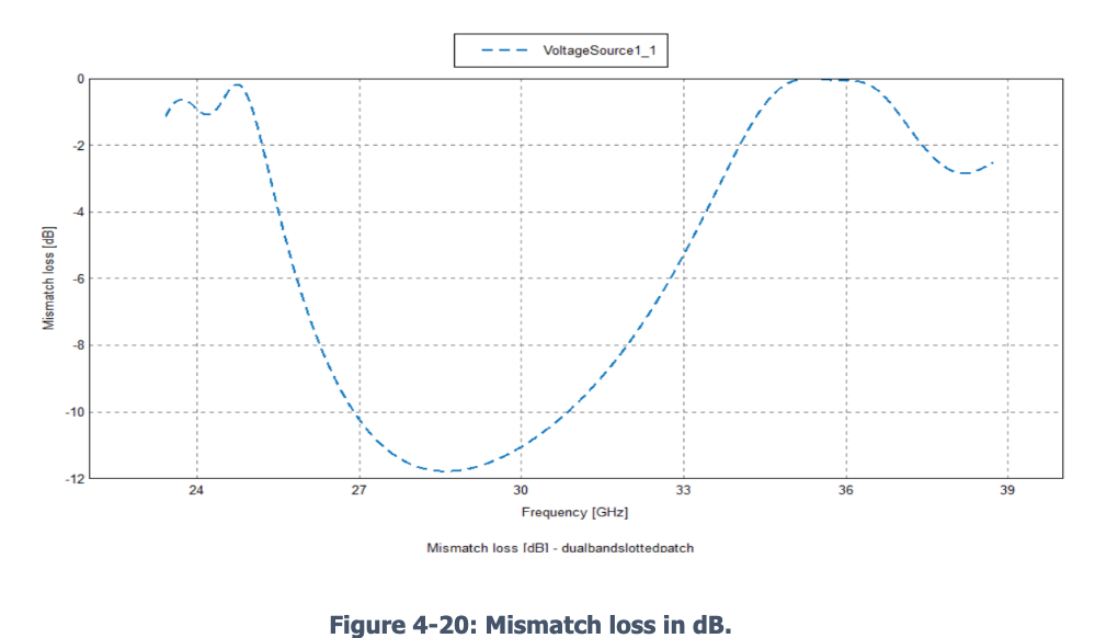
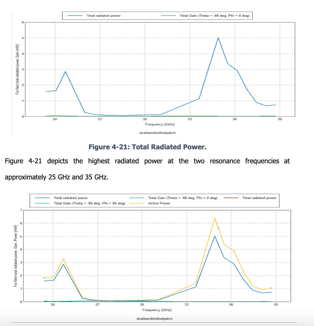
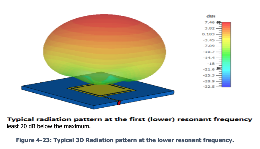
The designed antenna’s performance was evaluated in terms of return loss, radiation pattern, power radiated, Voltage Standing Wave Ratio (VSWR), impedance, and gain at both 26 and 36 GHz. The gain value was observed to be seven dBi at a lower resonant frequency and near to six dBi at the upper resonant frequency. The return loss matching was observed near -15 dB and near to -35 dB at the upper resonant frequency, indicating a solid match. The VSWR also follows the reflection coefficient, two at the lower resonance frequency and approximately one at the upper resonance frequency. The mismatch loss has a value of about 0.5 at lower resonance frequencies and almost zero at upper resonance frequencies. Hence, upper resonance depicts a better total power radiated (TRP) number. The radiation characteristics are somewhere in the middle of a wideband antenna and a narrowband antenna. The gain is not very high, a value of seven and six dBi at 25 and 36 GHz, respectively, so the beamwidth is approximately 800 at both resonances, while the side lobe level (SLL) is least 20 dB below the
maximum. The proposed slotted patch dual-band antenna exhibited excellent performance characteristics for 5G wireless communications at 26 and 36 GHz. It achieved good impedance matching, high radiation efficiency, and wide bandwidth in both frequency bands. Moreover, the compact size and ease of fabrication make it a suitable candidate for integration into compact and portable 5G devices.
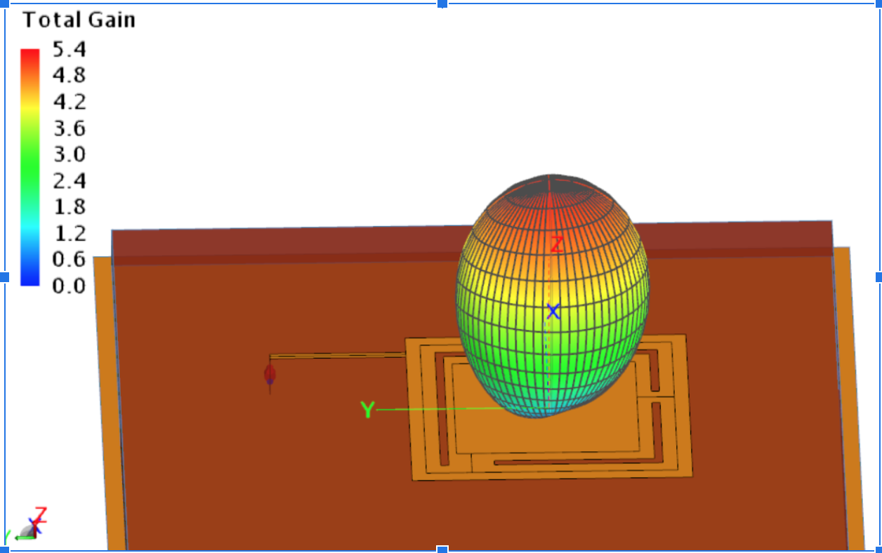


Height of substrate, h: Increasing h increases bandwidth. Rule of thumb. An antenna having more space in spherical volume will have higher bandwidth. This is analogous to a dipole; making dipole thick, increasing the diameter, increases bandwidth.
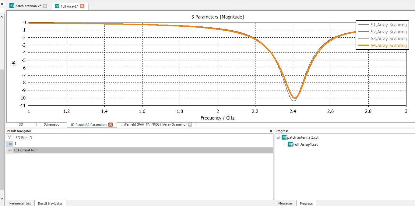
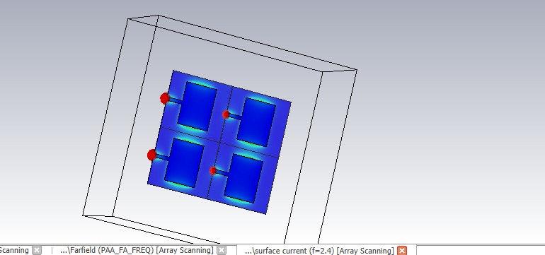
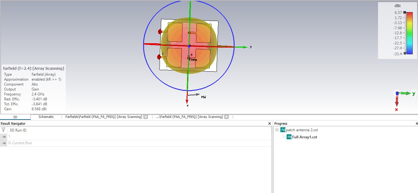
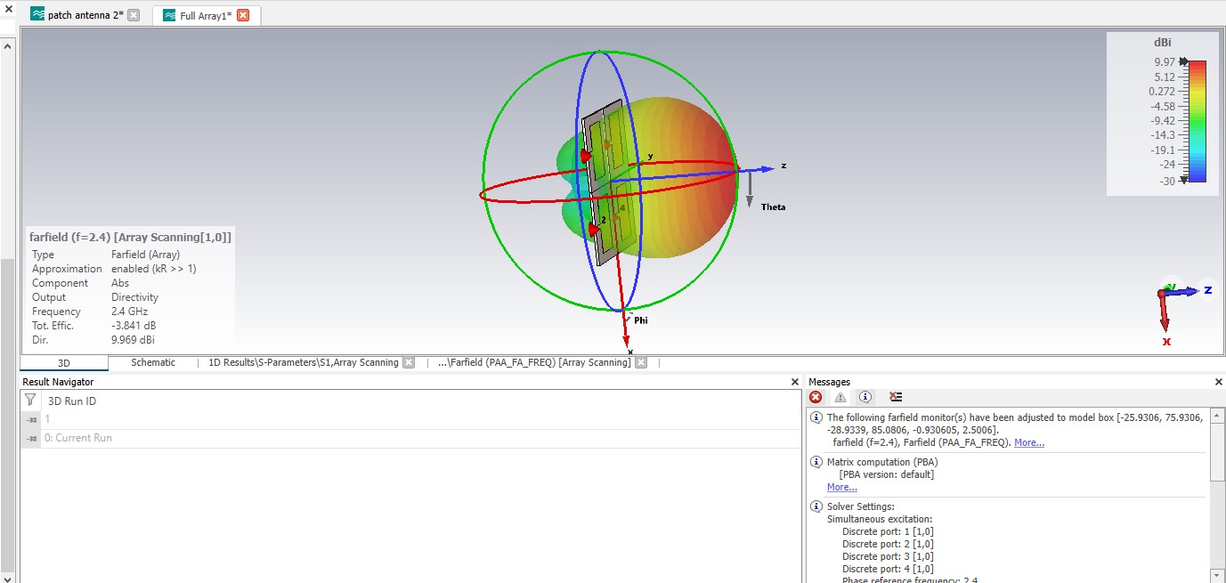
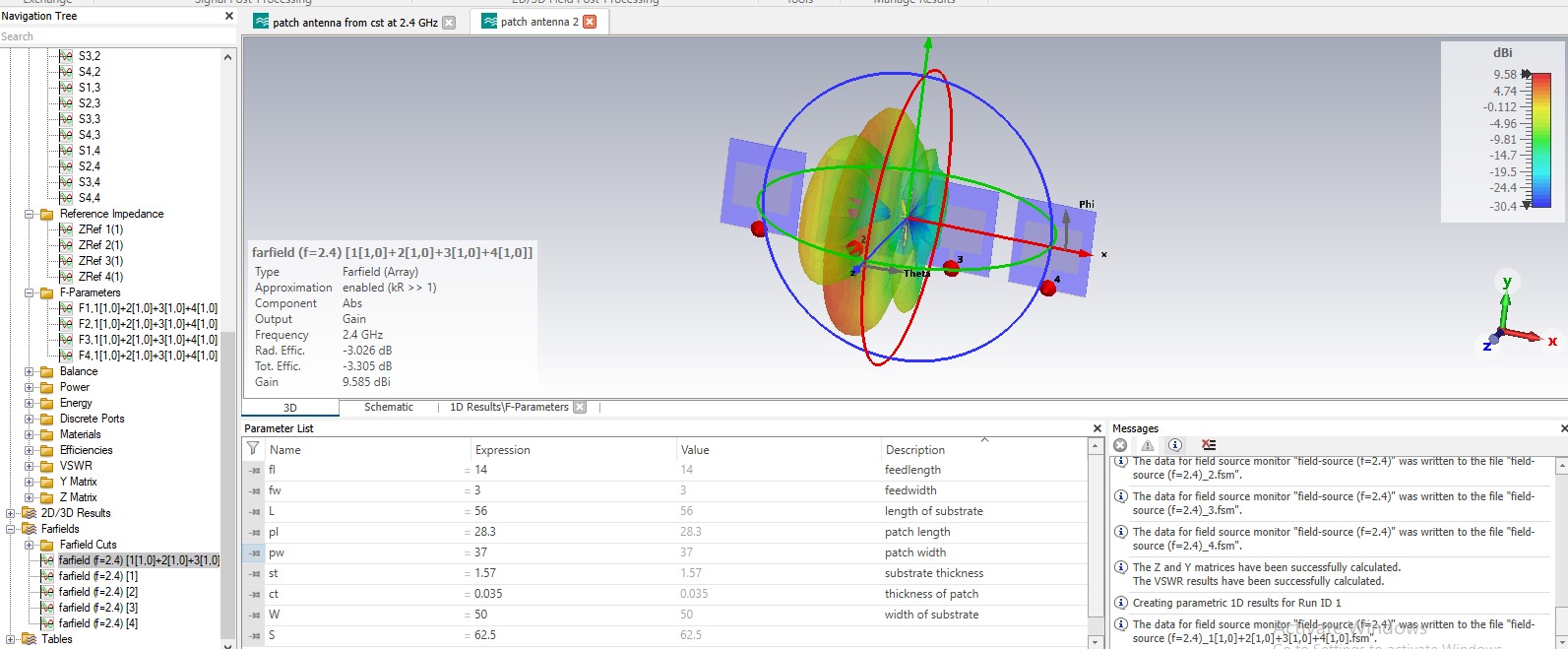
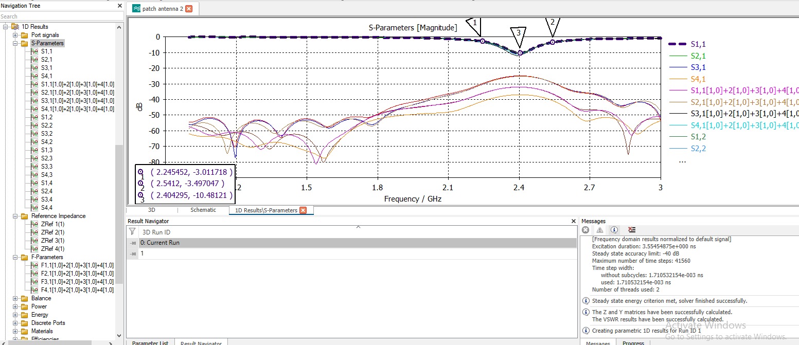
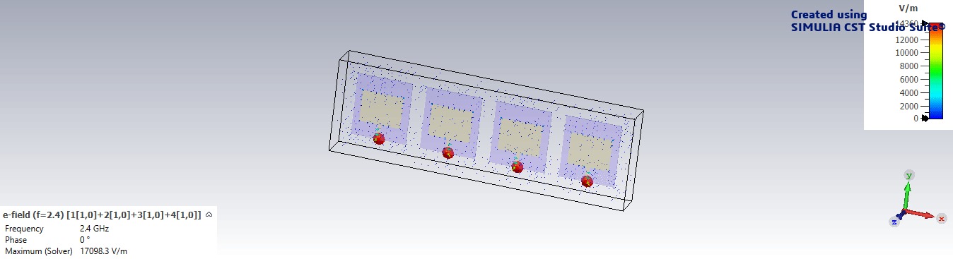
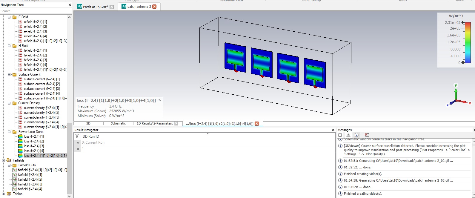
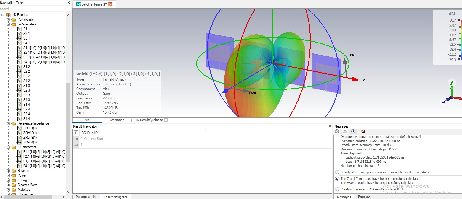
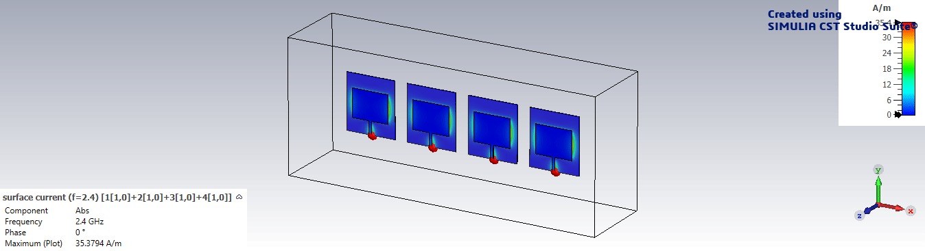
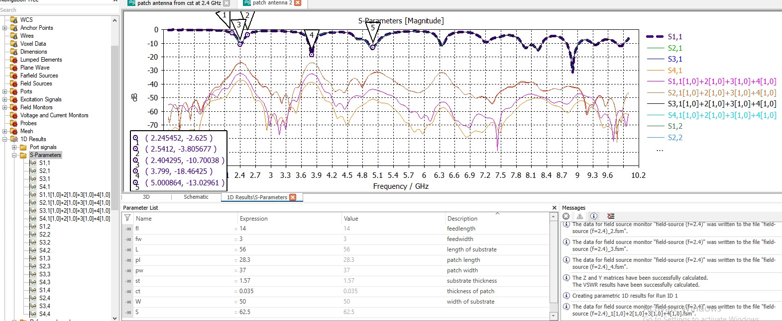
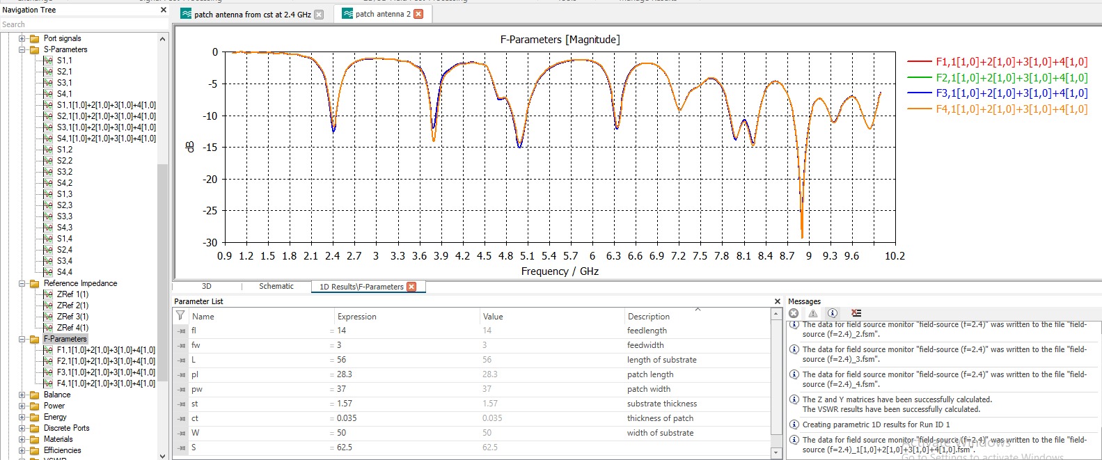
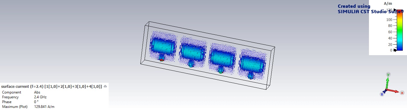
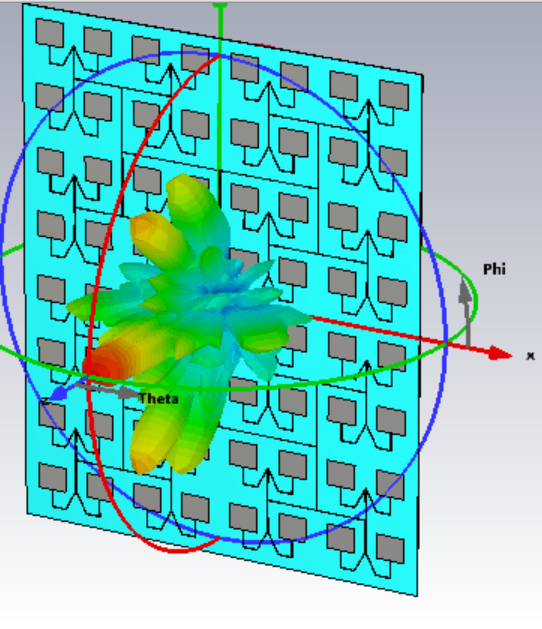
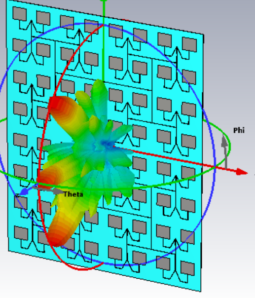
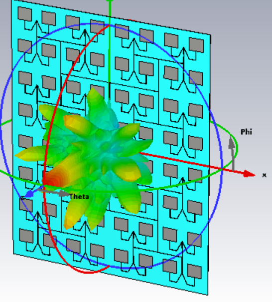
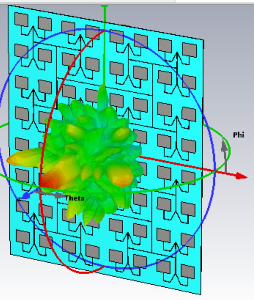
Patch antenna design and conversion into 2*2 and 4*1 patch array.
A patch antenna with a feed straight on the patch was designed at 2.4 GHz (no insets). The single element was converted into an array in two different configurations. Both configurations achieved a gain of 9.585 dBi and 9.98 dBi.
Lessons learned from patch antenna design.
Length, L, controls resonant frequency. Longest length corresponds to the lowest frequency of operation.
Width, W, controls the input impedance and radiation pattern. Wider the patch, lower the input impedance is.
the permitivity, Er, of the substrate controls the fringing fields, lower permittivities have wider fringes, and hence better radiation patterns. decreasing the perittivty also increases the antenna bandwidth. The efficiency is also increased with lower values of permittivity. Impedance increases with higher permittivity.
Higher value of permittivity shrinks the antenna, In Mobile phones, the space is tight, hence designers can use very high values of permittivity.
If permittivity is increased by 4, the required length decreases by a factor of 2. Equations available at: https://www.antenna-theory.com/antennas/patches/patch4.php
Using high permittivity is frequntly exploited in antenna miniaturization.
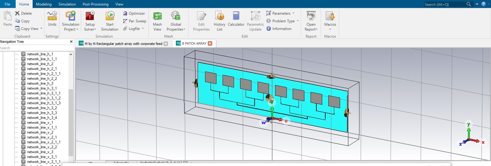
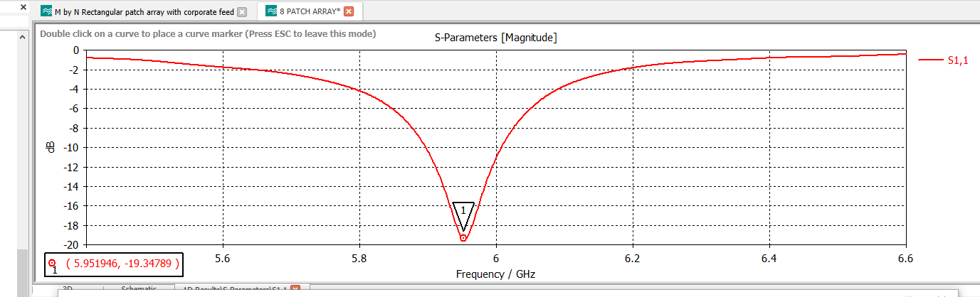
8*1 Patch array with corporate feed
The design of an N × 1 patch antenna array involves two main aspects: the design of the individual patch elements and the microstrip feed network that excites them. The dimensions of a single resonant patch are primarily determined by the substrate properties, while the characteristic impedance of the feed lines is constrained by practical fabrication considerations.
For instance, if the required characteristic impedance becomes significantly higher than about 100 Ω, the resulting microstrip line widths may become too narrow to fabricate reliably through standard etching processes. This limitation depends on factors such as substrate thickness and relative permittivity. On the other hand, if the input port resistance is selected too low, the microstrip lines may become excessively wide, which can also be impractical from a layout and integration perspective.
If the design does not require a specific substrate, it is advisable to use typical commercial substrate parameters, such as a relative permittivity around 2.2, with a substrate thickness approximately 5% of the wavelength inside the dielectric medium. However, in microstrip arrays with coplanar corporate feed networks, selecting the substrate permittivity involves a trade-off between competing requirements. Patch antennas generally achieve higher bandwidth with low permittivity substrates and thicker dielectric layers, whereas the feed network performs better when the guided waves are tightly confined and non-radiating, which favors higher permittivity and thinner substrates. Therefore, substrate selection must balance these conflicting design goals.
Several design parameters can be adjusted to optimize antenna performance:
Important Note:
Very thin substrates tend to introduce higher copper losses, which can reduce antenna efficiency. Conversely, thicker substrates with high permittivity may degrade antenna performance due to the excitation of surface waves, which can increase unwanted radiation and reduce radiation efficiency.
Patch length adjustment:
The resonant frequency (or center frequency) of each patch element can be shifted by modifying the patch length.Patch width adjustment:
The input resistance of a single resonant patch can be reduced by increasing the patch width. However, this adjustment should be limited so that the ratio Wp/Lp does not exceed 2, because the aperture efficiency begins to degrade when the width becomes too large relative to the length. This behavior is documented in antenna literature such as Balanis.Inset feed tuning:
A more effective approach to controlling the input impedance of a patch is to use an inset feed configuration instead of a simple edge feed. This allows finer impedance tuning without excessively altering the patch geometry.Bandwidth improvement:
The antenna bandwidth can be increased by increasing the substrate thickness and/or reducing the substrate permittivity. However, these changes will also influence the resonant frequency and impedance matching, so they must be applied carefully.Feed network impedance matching:
The overall input impedance of the array can be adjusted by modifying the width and length of the input matching section within the corporate feed network.
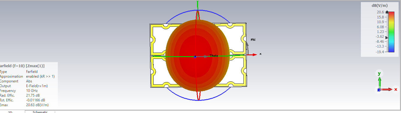
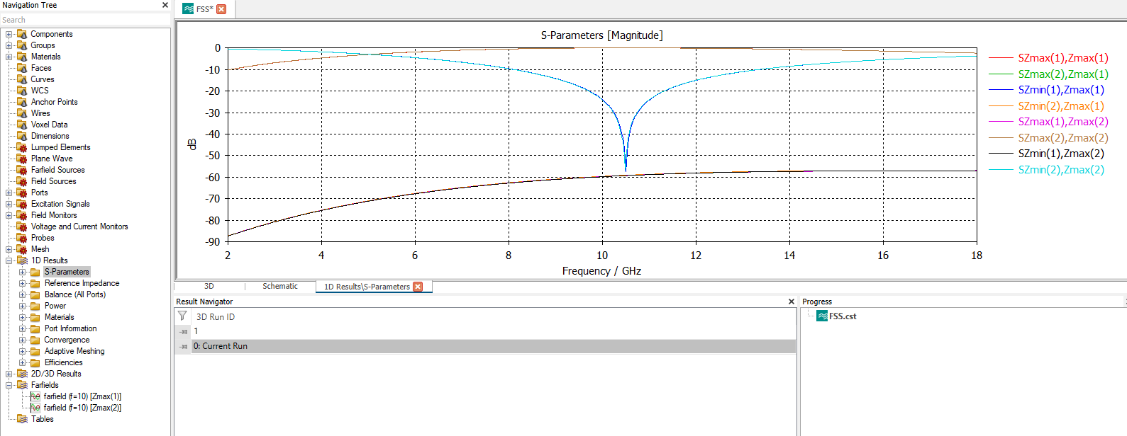
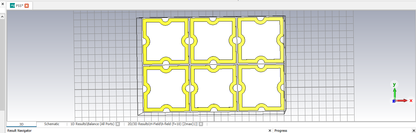
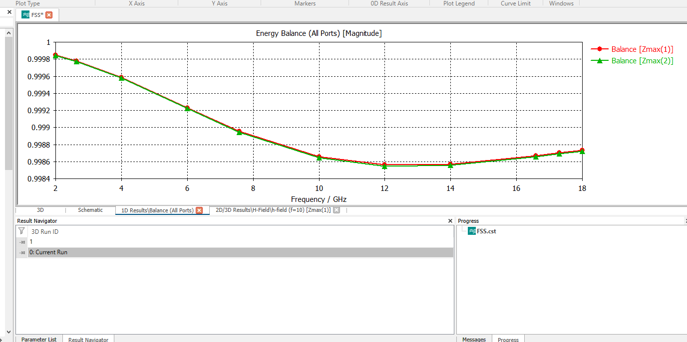
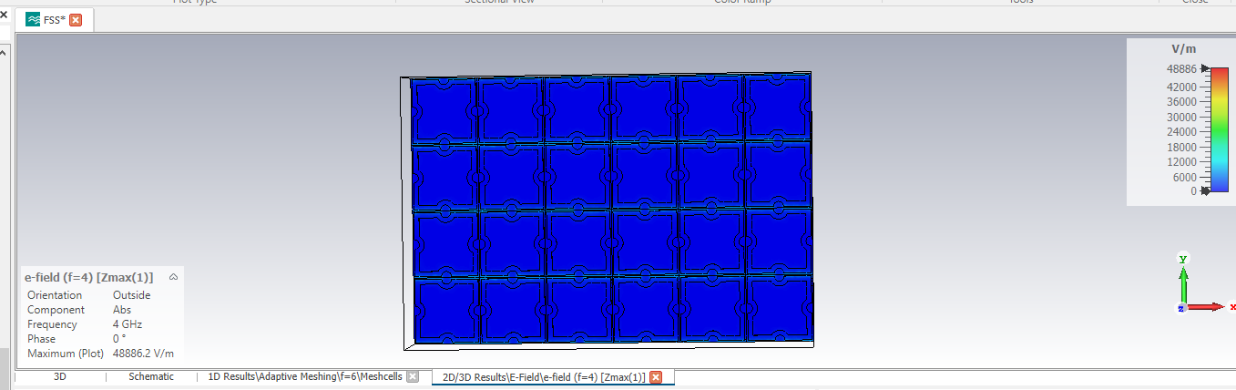
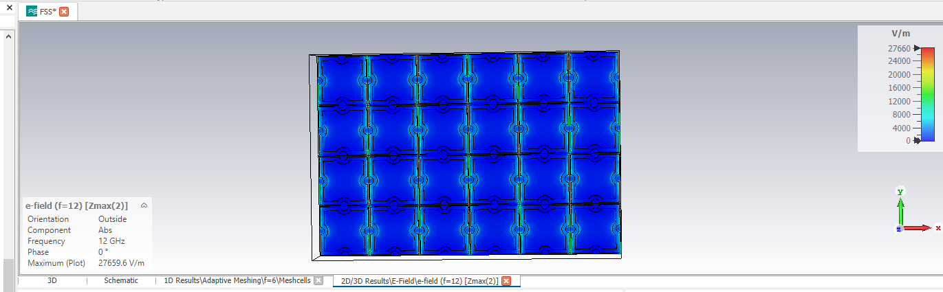
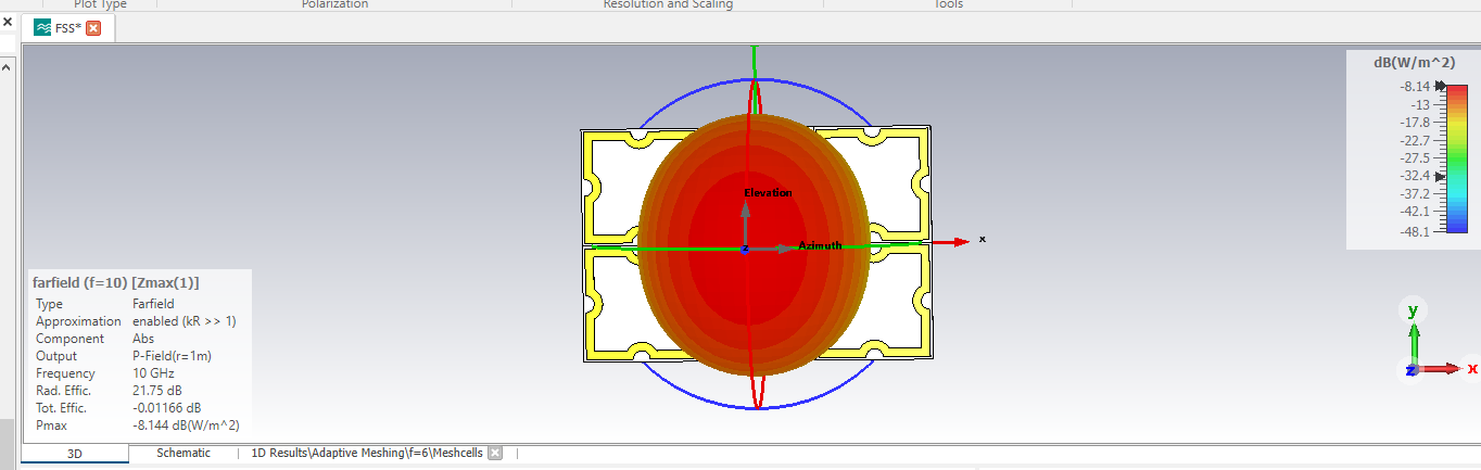
Freqeuncy Selective Surface (FSS) unit cell simulation in CST.
FSS are periodic structures that filter EM waves. They allow certain frequencies to pass or reflect based on design. They are used in antennas, radomes, Stealth technology and EM shielding. FSS consists of repetitive patterns (patches, slots, and dipoles). They act like a spatial filter. Behaviour depends upon the shape of the elements and their periodicity (spacing).
Common FSS structures: Square loop: Useful for bandpass filtering.
Dipole array: Simple bandstop behaviour.
Slot array: Slots in a conductive sheet allow transmission at certain frequencies. Jerusales Cross: Complex structures for multiband bahviour.
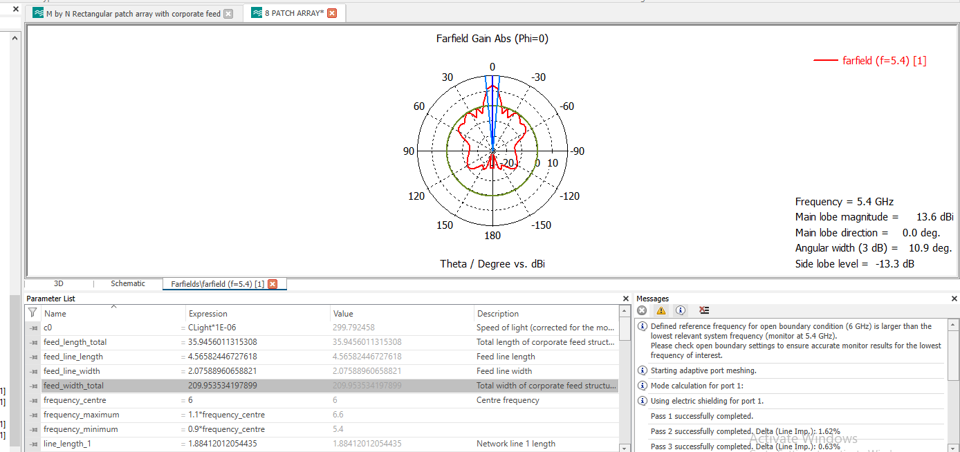
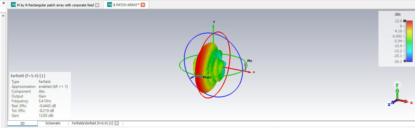
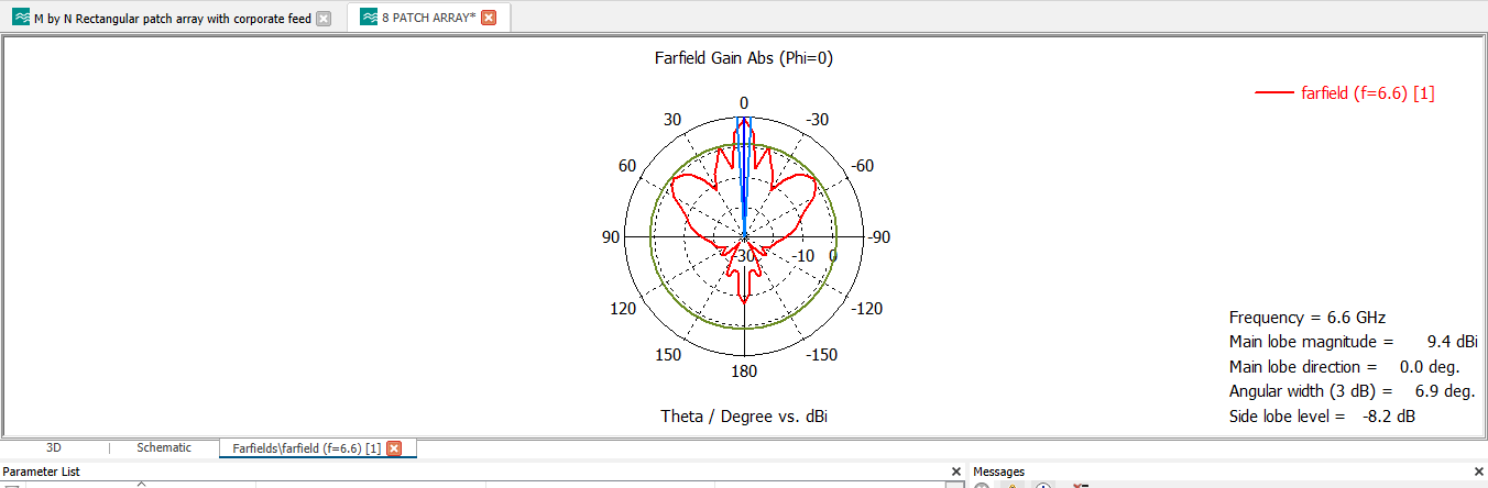
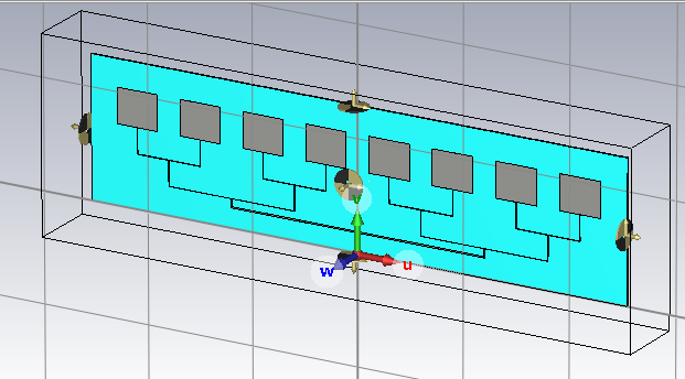
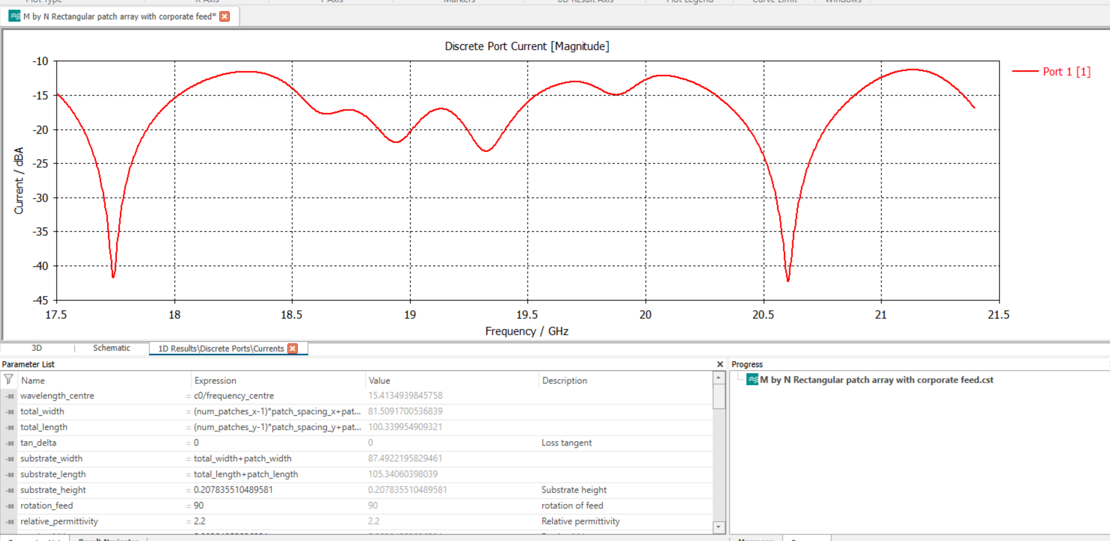
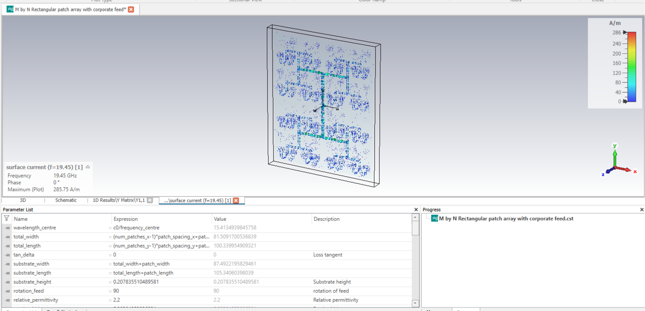
M by N (8*8) rectangulat patch array withcorporate feed at 19.13 GHz.
A rectangular microstrip patch antenna array is widely used to achieve higher gain, improved directivity, and better control over the radiation pattern compared to a single patch element. In an 8 × 8 planar array, a total of 64 identical patch elements are arranged in a rectangular grid. Each element acts as an individual radiator, and when excited with the proper phase and amplitude distribution, the array radiates coherently, producing a highly directive beam with increased effective aperture.
The operation of microstrip patch antennas is based on the fringing fields that occur at the edges of the rectangular patch. When the patch dimensions are approximately half a wavelength in the dielectric medium, the antenna resonates in the fundamental TM10 mode, producing broadside radiation. In an array configuration, the individual patch elements are typically spaced around 0.5λ (in free space) to minimize mutual coupling and prevent the formation of grating lobes while maintaining constructive interference in the desired direction.
To distribute RF power uniformly to all 64 elements, a corporate feed network is commonly employed. A corporate feed is a parallel power division network consisting of multiple stages of T-junction power splitters. The input power is progressively divided into equal portions until each patch element receives approximately the same excitation. For an 8 × 8 array, the feed network typically requires several cascading stages of 1-to-2 power dividers, forming a tree-like structure that ensures equal amplitude and phase at each element.
Impedance matching is a critical aspect of corporate feed design. At each power division junction, the characteristic impedance of the transmission lines must be adjusted to maintain proper matching and minimize reflections. This is often achieved using quarter-wave impedance transformers or appropriately chosen microstrip line widths. For example, when a transmission line splits into two equal branches, the impedance of each branch is typically increased by a factor of sqrt(2) to maintain the desired input impedance at the junction.
The corporate feed architecture offers several advantages. It provides precise control of amplitude and phase, which is essential for beamforming and array pattern synthesis. It also ensures equal excitation of all elements, enabling the array to produce a strong and well-defined main beam. However, this approach can increase feed network complexity, insertion losses, and physical layout size, particularly for large arrays such as the 8 × 8 configuration.
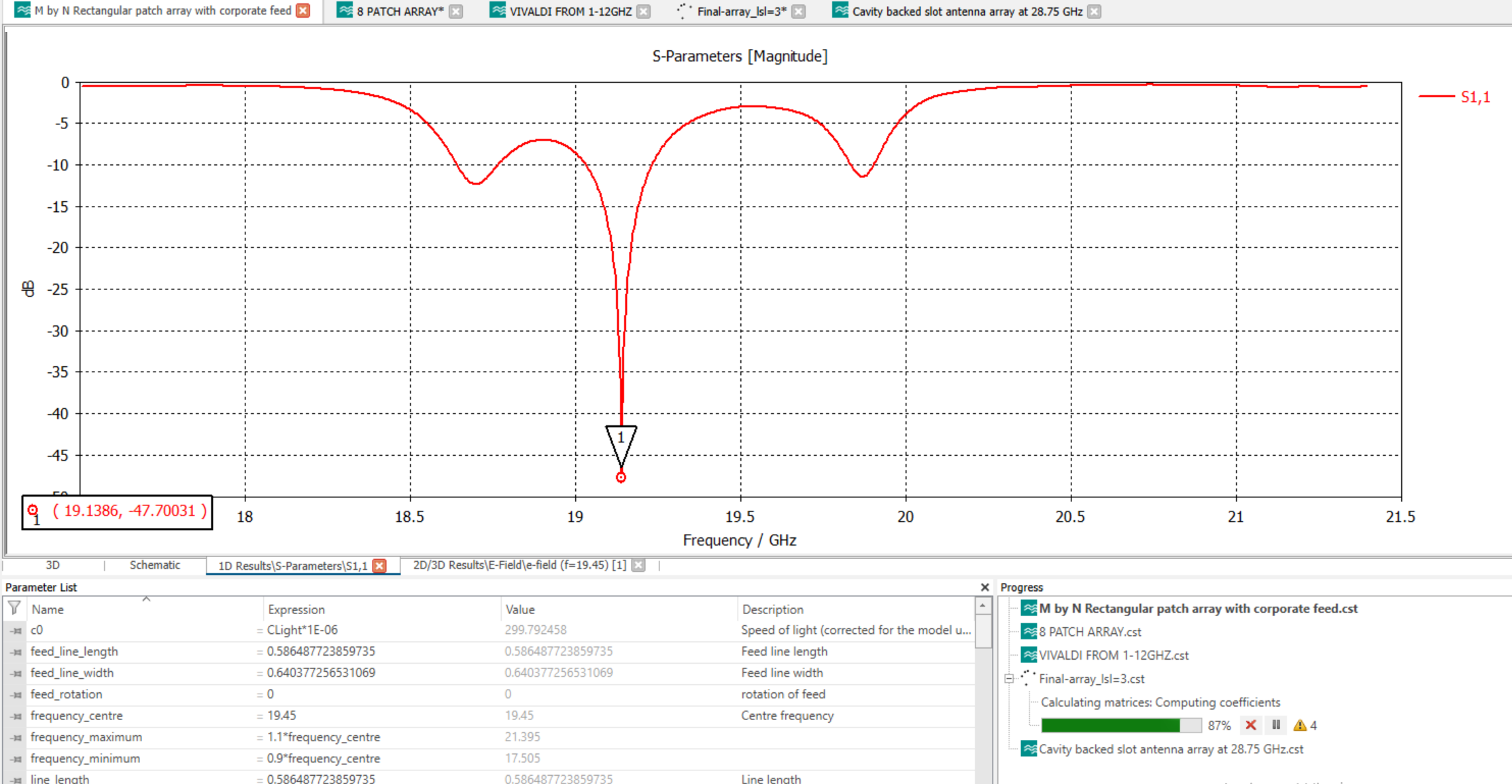
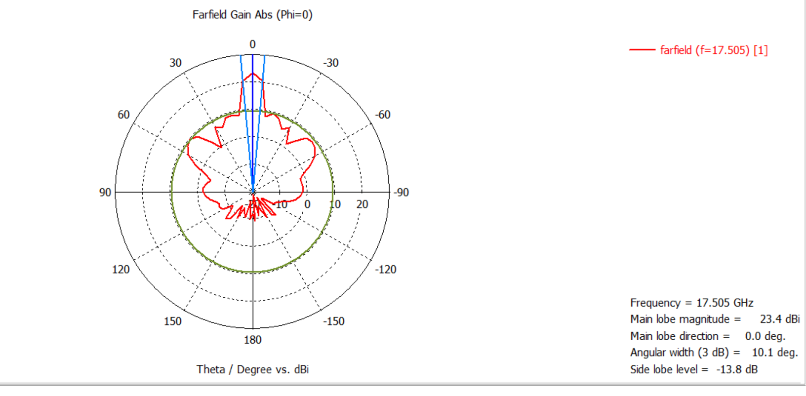
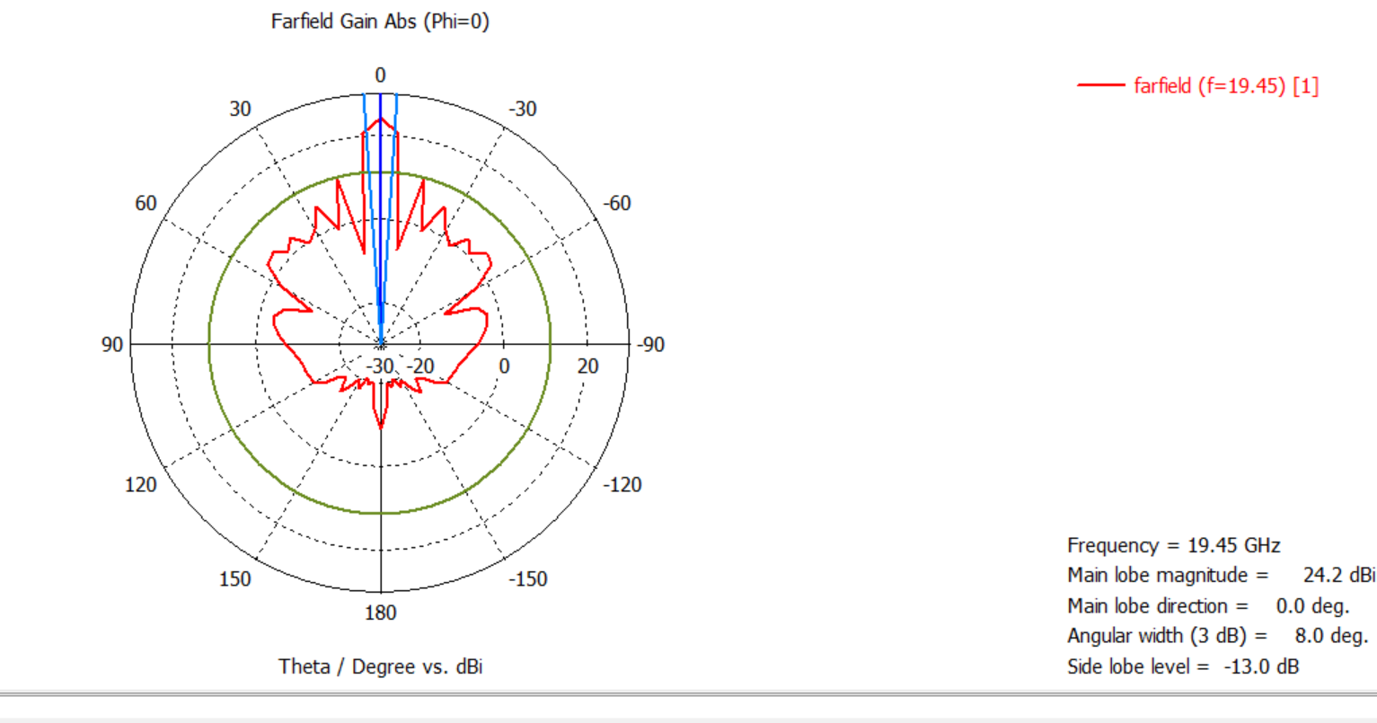
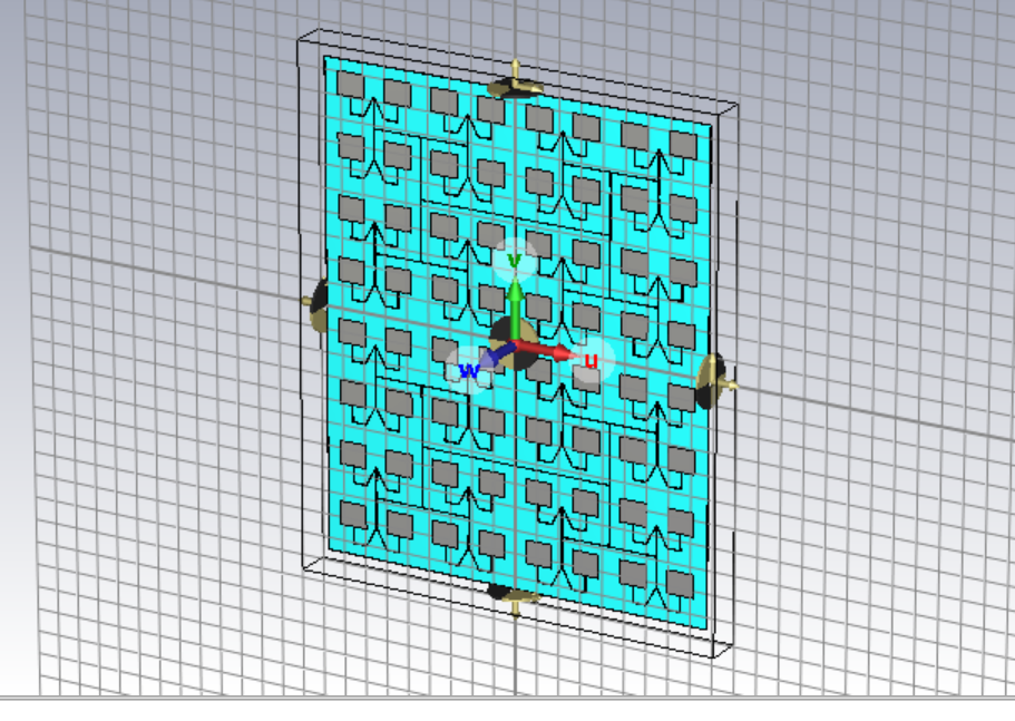
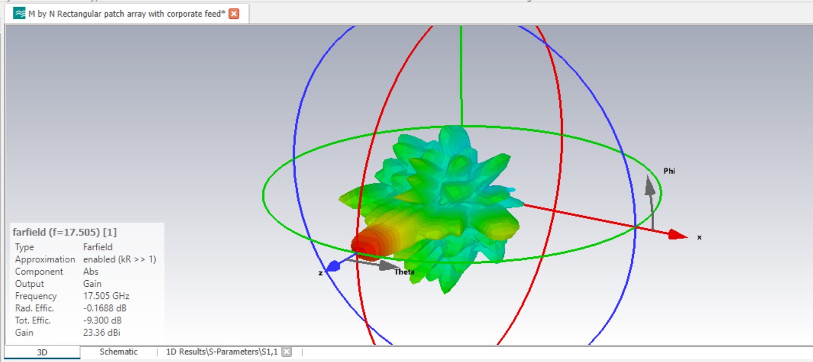
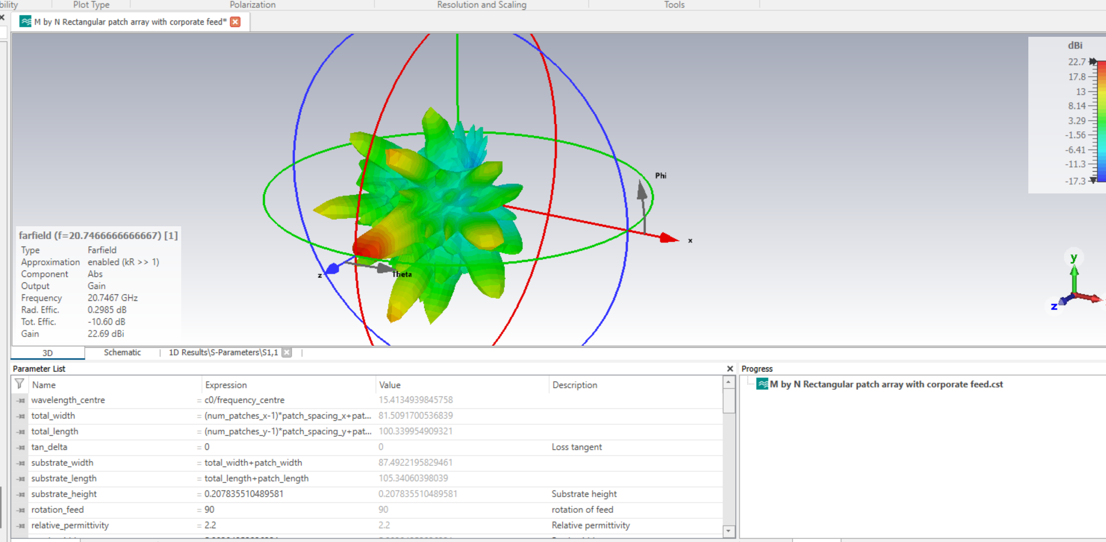
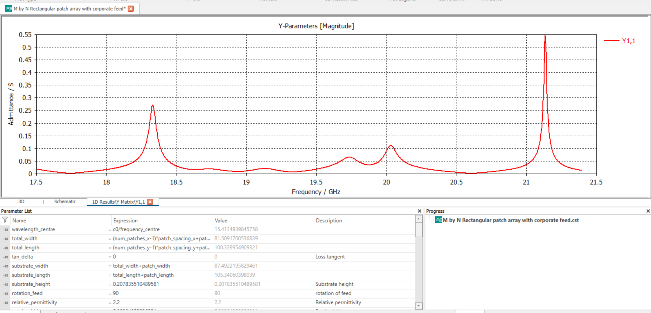
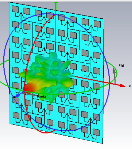
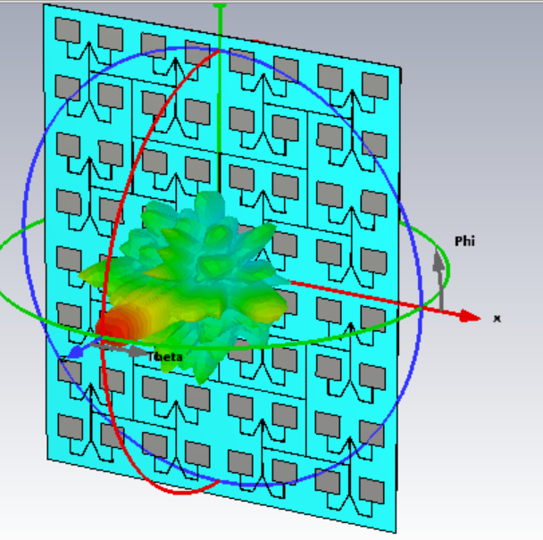
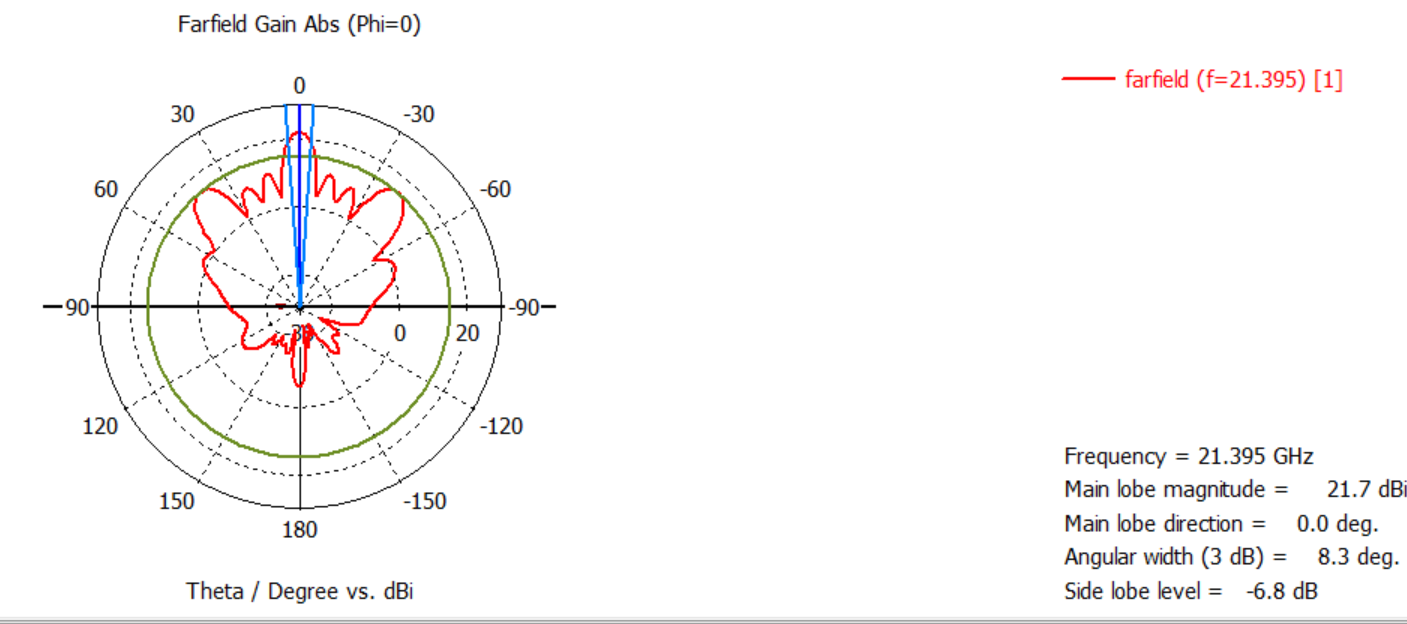
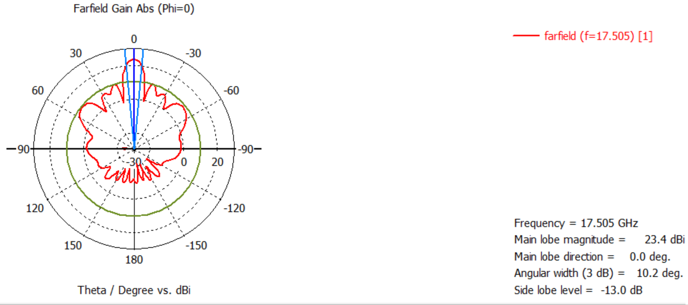
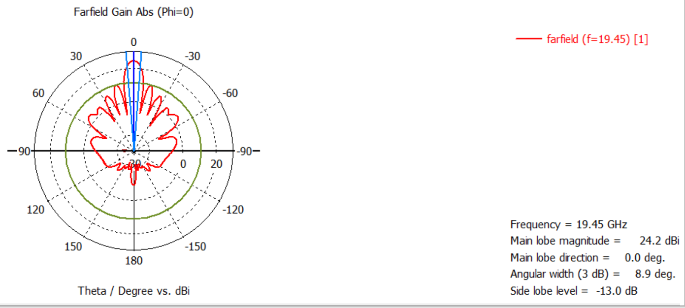
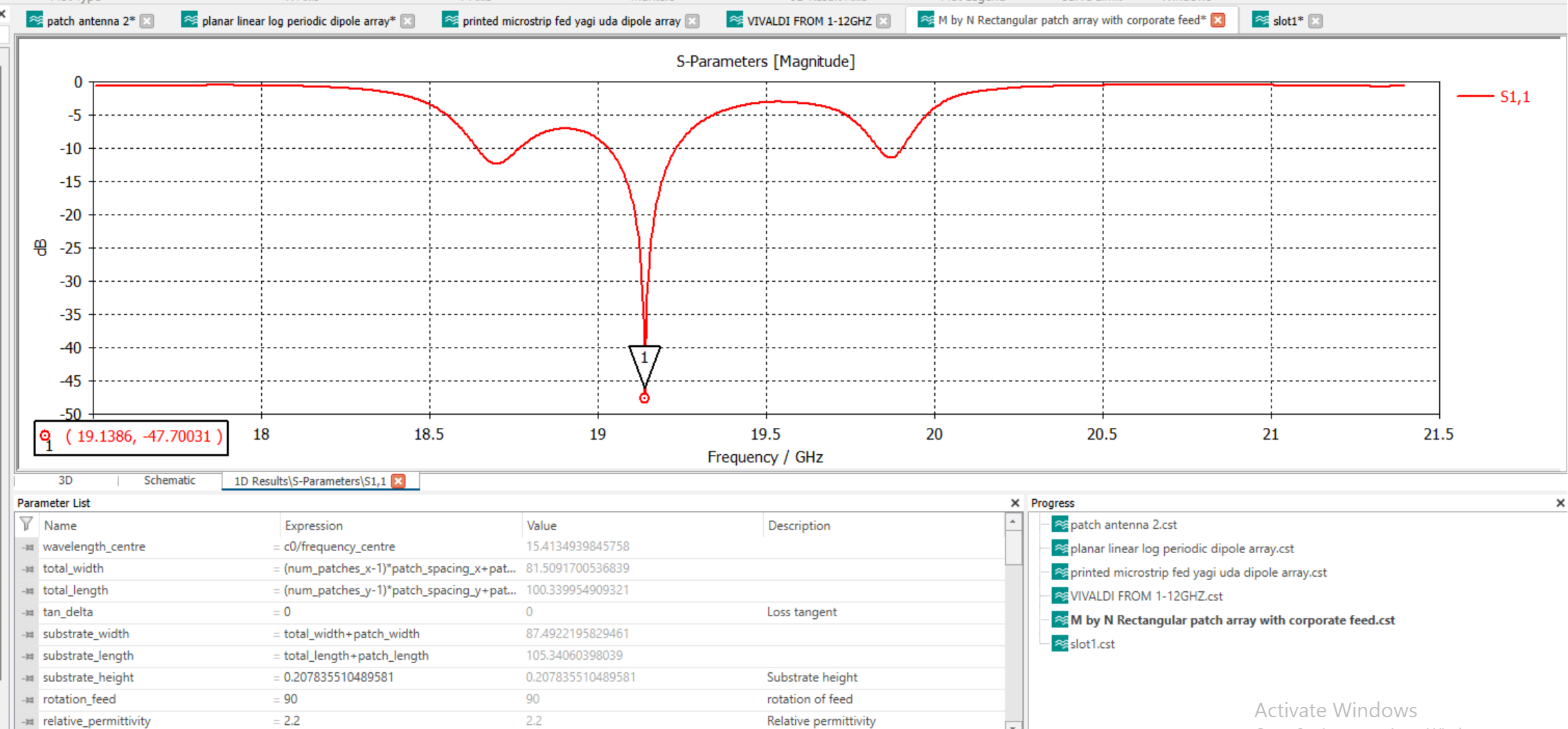
In the designed 8 × 8 rectangular patch array, the corporate feed network distributes power to all 64 radiating elements, enabling the array to achieve significantly higher gain and narrower beamwidth compared to a single patch antenna. Such arrays are commonly used in applications requiring high directivity and efficient radiation, including radar, satellite communications, and wireless communication systems.
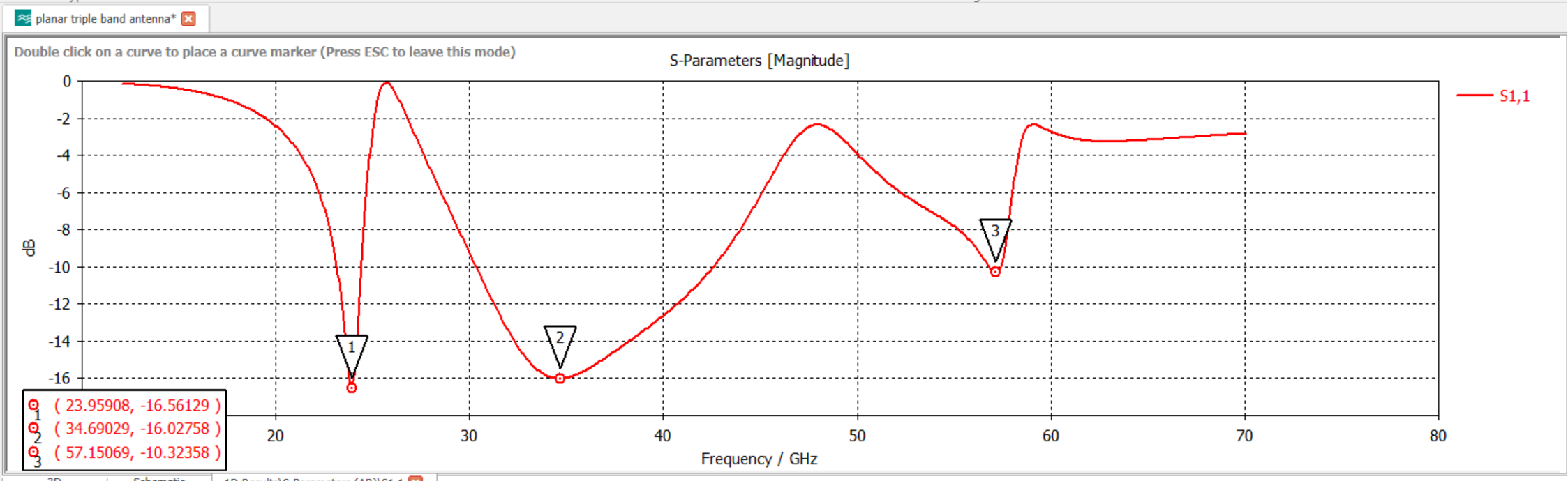
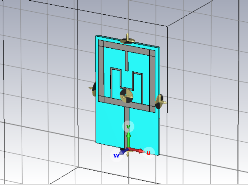
Additionally, a narrow rectangular strip extending from the upper region of the peripheral rectangular ring is included in the design. This strip acts as a parasitic coupling element, further modifying the electromagnetic field distribution across the patch surface. By introducing this additional resonant path, the antenna can support higher-order modes and improve the impedance characteristics at the upper operating frequency band.
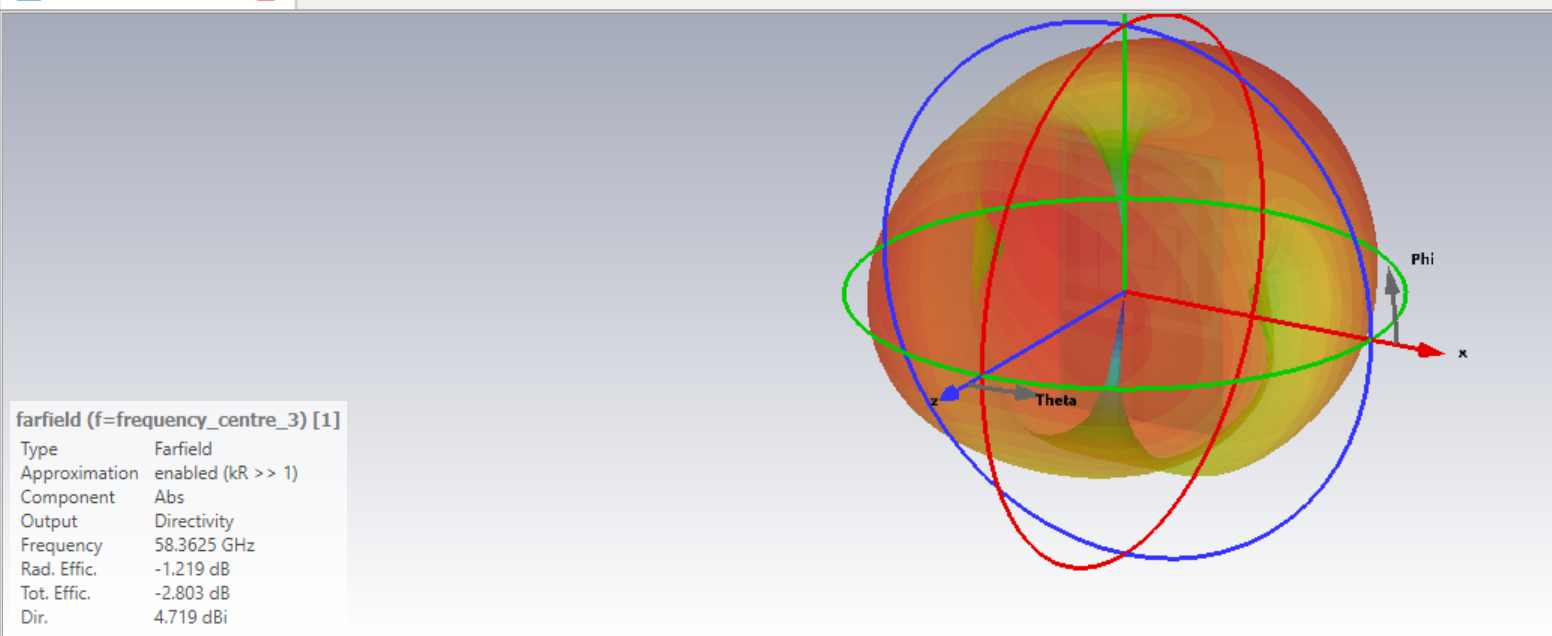
Overall, the combination of the feed structure, the peripheral rectangular ring elements, the M-shaped conductive path, and the narrow coupling strip enables the antenna to support three distinct resonant modes. These structural features collectively control the surface current distribution, effective electrical length, and coupling mechanisms, allowing the antenna to operate efficiently at 23.95 GHz, 34.69 GHz, and 57.15 GHz while maintaining a compact planar geometry suitable for millimeter-wave applications.
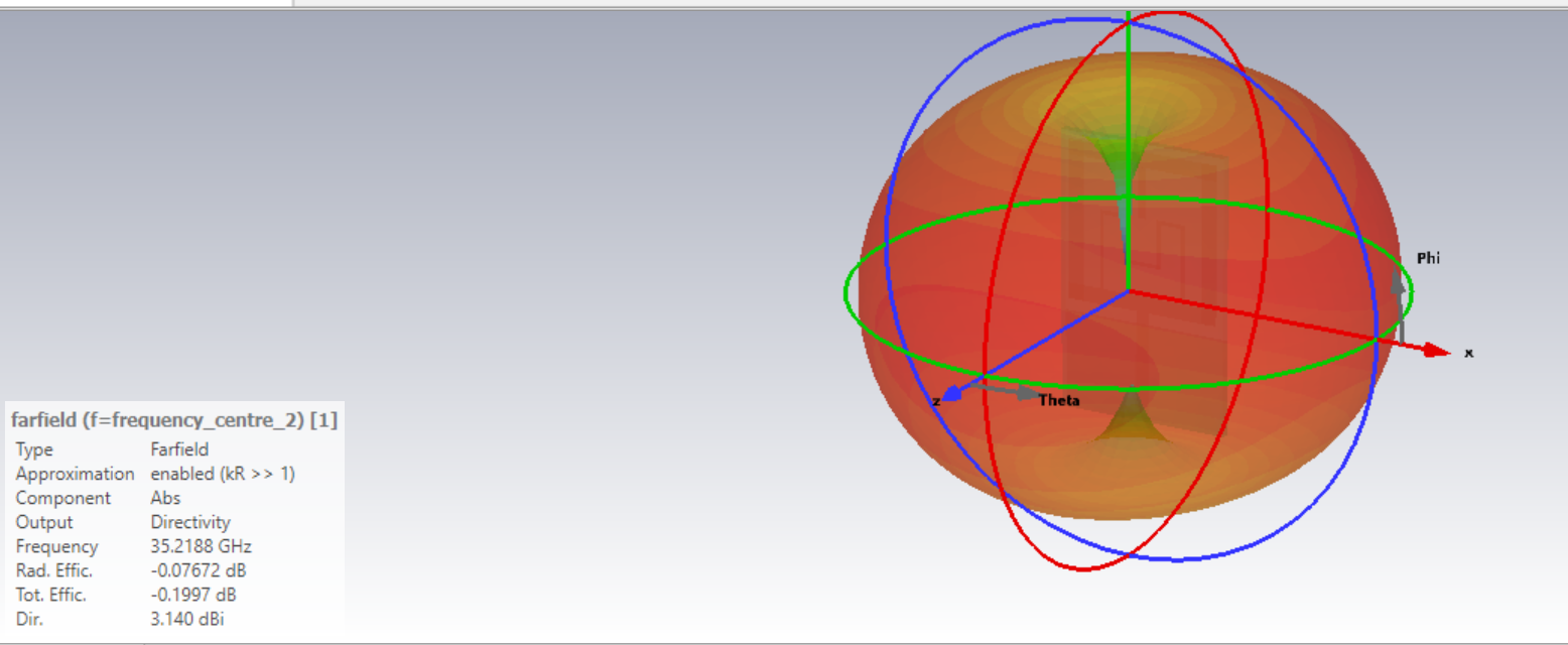
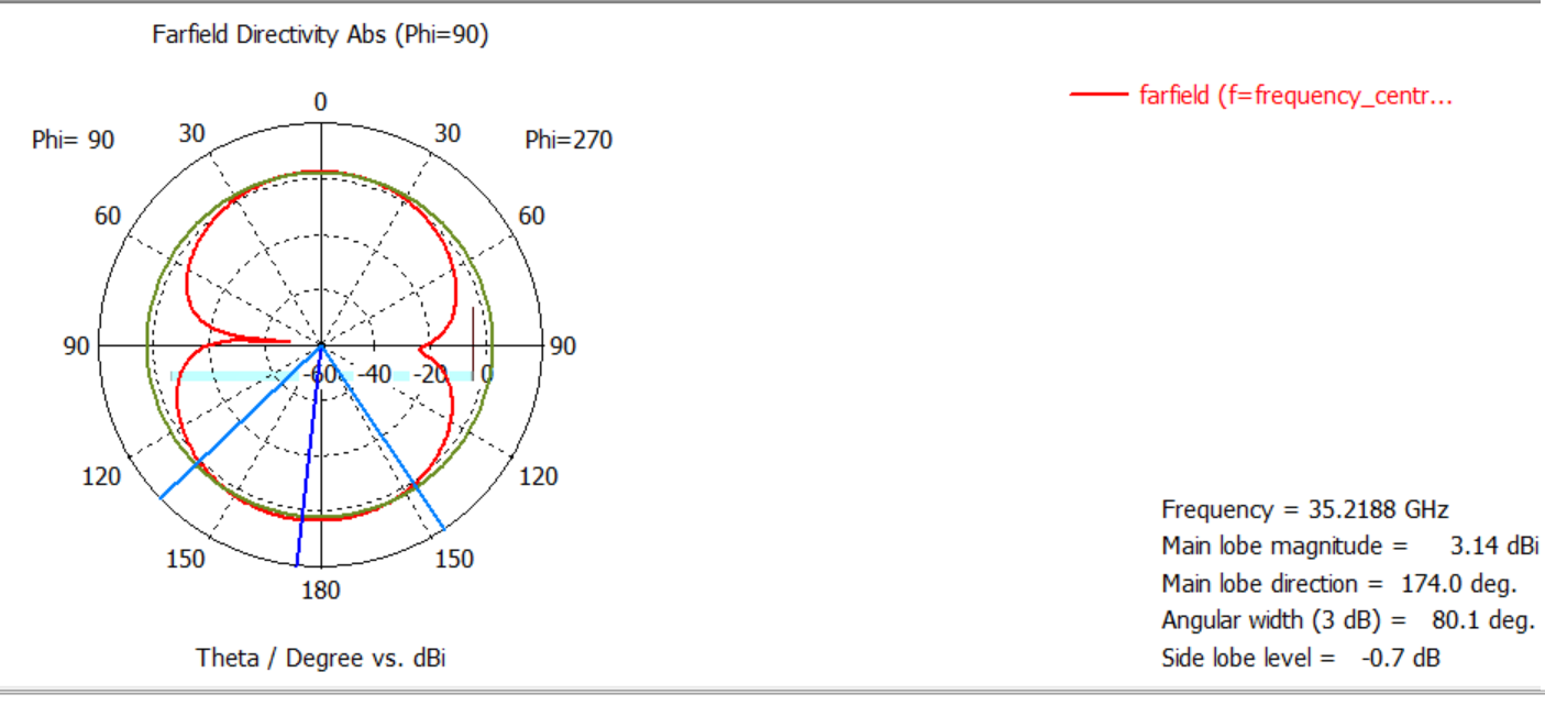
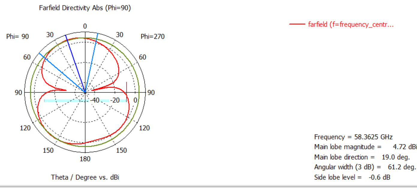
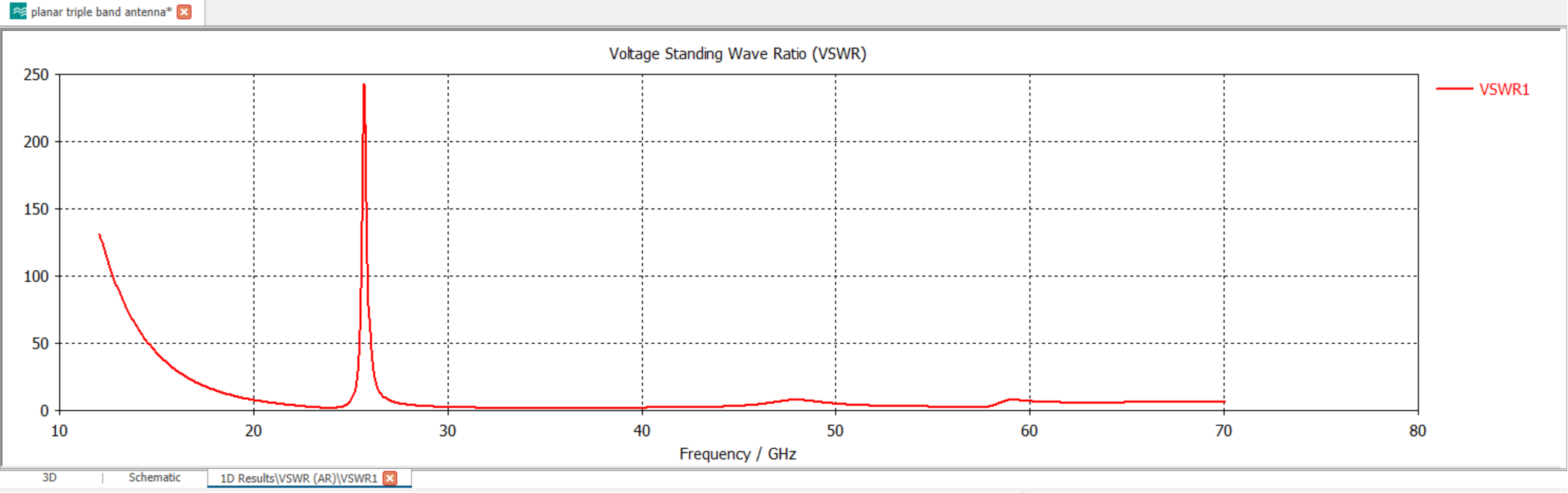
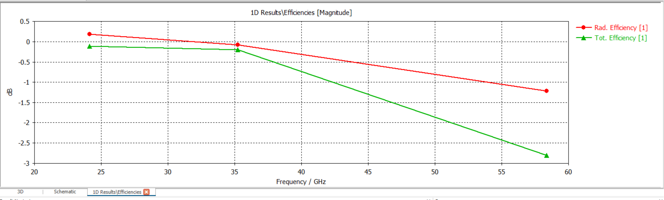
Planar Triple band antenna at 24, 34.7, and 57.15 GHz.
The proposed antenna is a planar microstrip patch antenna designed to operate at three millimeter-wave frequencies: 23.95 GHz, 34.69 GHz, and 57.15 GHz. Microstrip patch antennas are widely used at millimeter-wave frequencies because of their low profile, ease of fabrication, planar geometry, and compatibility with integrated circuits. The basic operating principle of a rectangular patch antenna relies on the excitation of resonant cavity modes, where radiation occurs due to fringing fields at the patch edges. By modifying the geometry of the radiating structure and the surrounding conductive features, multiple resonant modes can be generated, enabling multi-band operation.
In the proposed design, the antenna is excited through a microstrip feed line, which delivers RF energy to the radiating structure. Immediately after the feed region, four narrow rectangular metallic sections are placed around the periphery of the substrate area. These rectangular sections form a ring-like conductive boundary near the edges of the structure. This configuration behaves as a parasitic resonant structure and surface current guide, which modifies the current distribution on the antenna surface. As a result, additional resonant paths are introduced, helping to support multiple operating frequencies.
Starting from the feed region, an M-shaped conductive structure is formed using several narrow rectangular segments. This structure increases the effective current path length and introduces additional discontinuities in the current flow. Such geometrical perturbations create multiple resonant modes, which contribute to the generation of the different operating frequency bands. The M-shaped configuration also enhances impedance matching by redistributing the surface currents and coupling energy more efficiently between the feed line and the radiating sections.
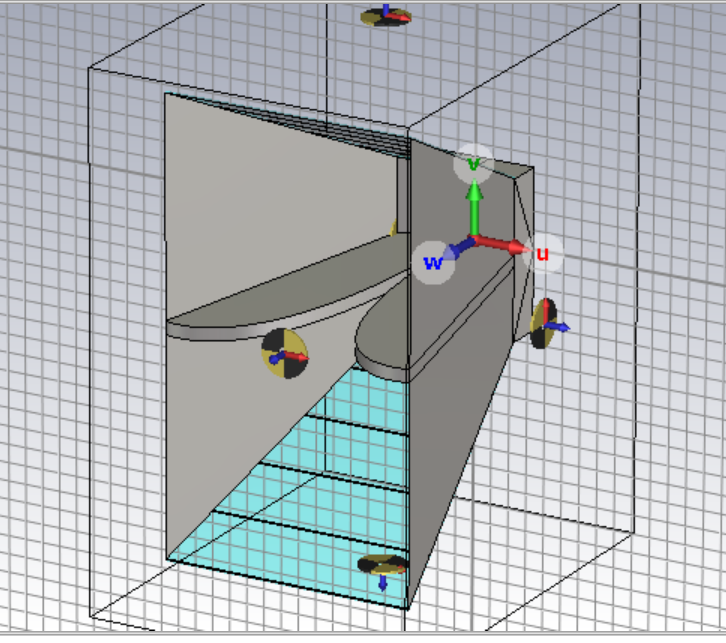
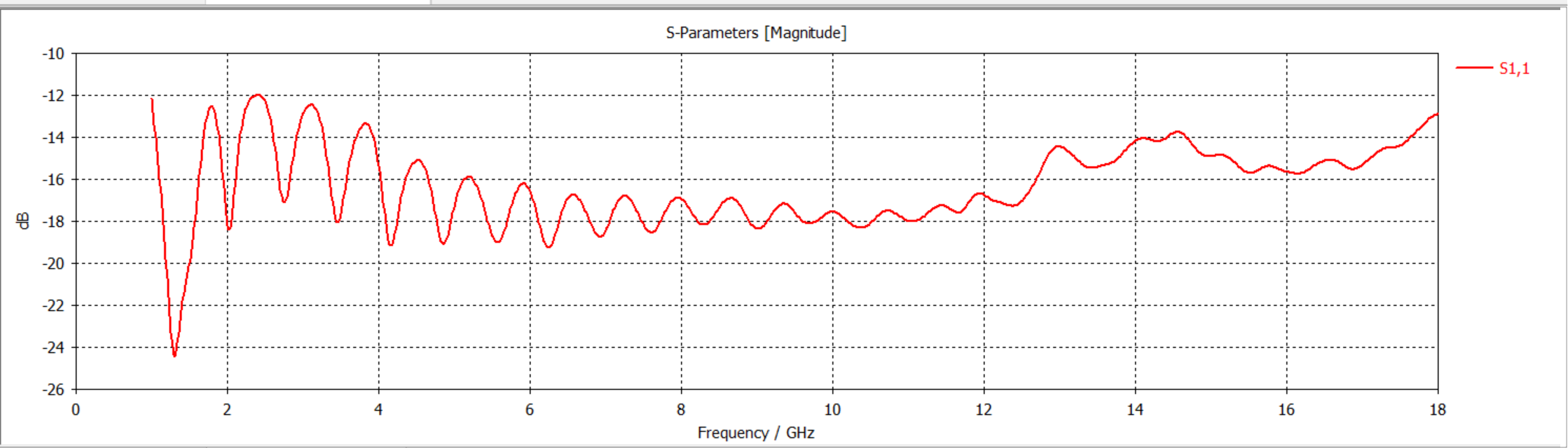
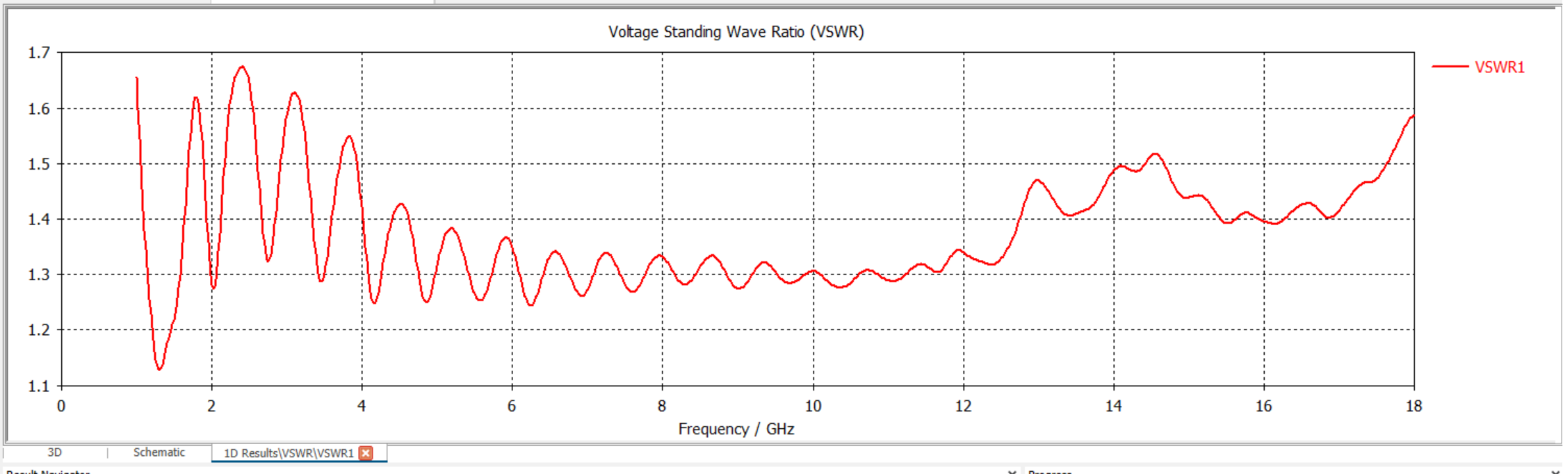
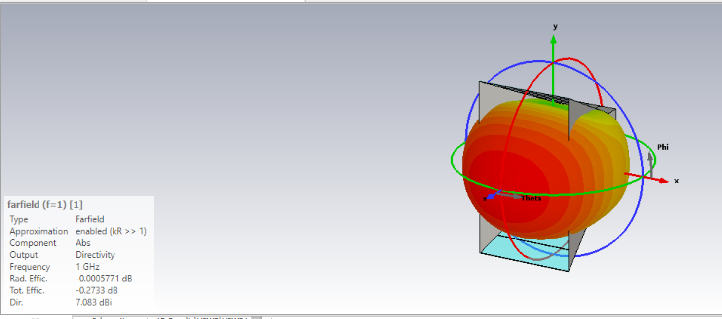
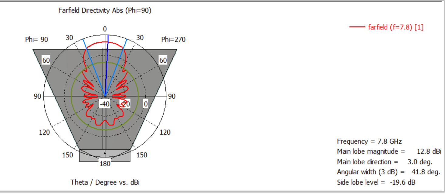
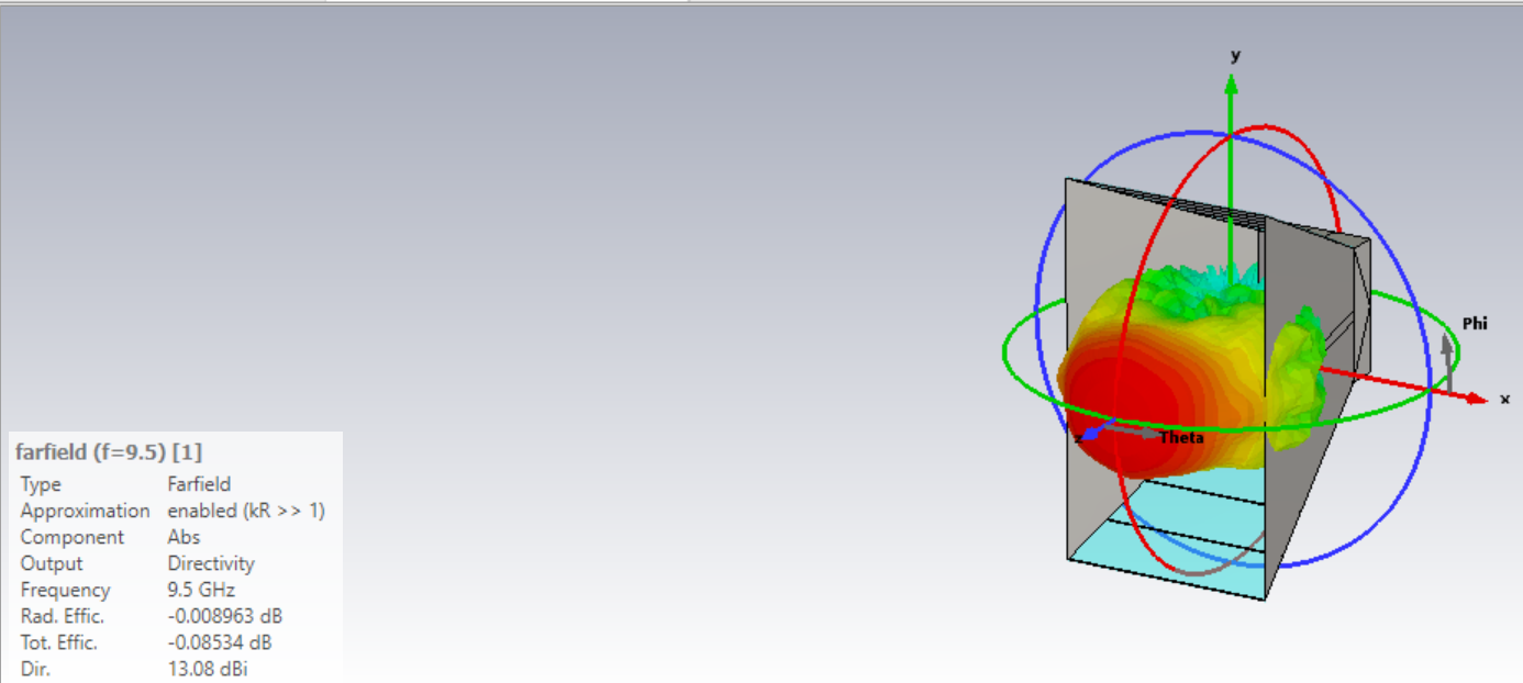
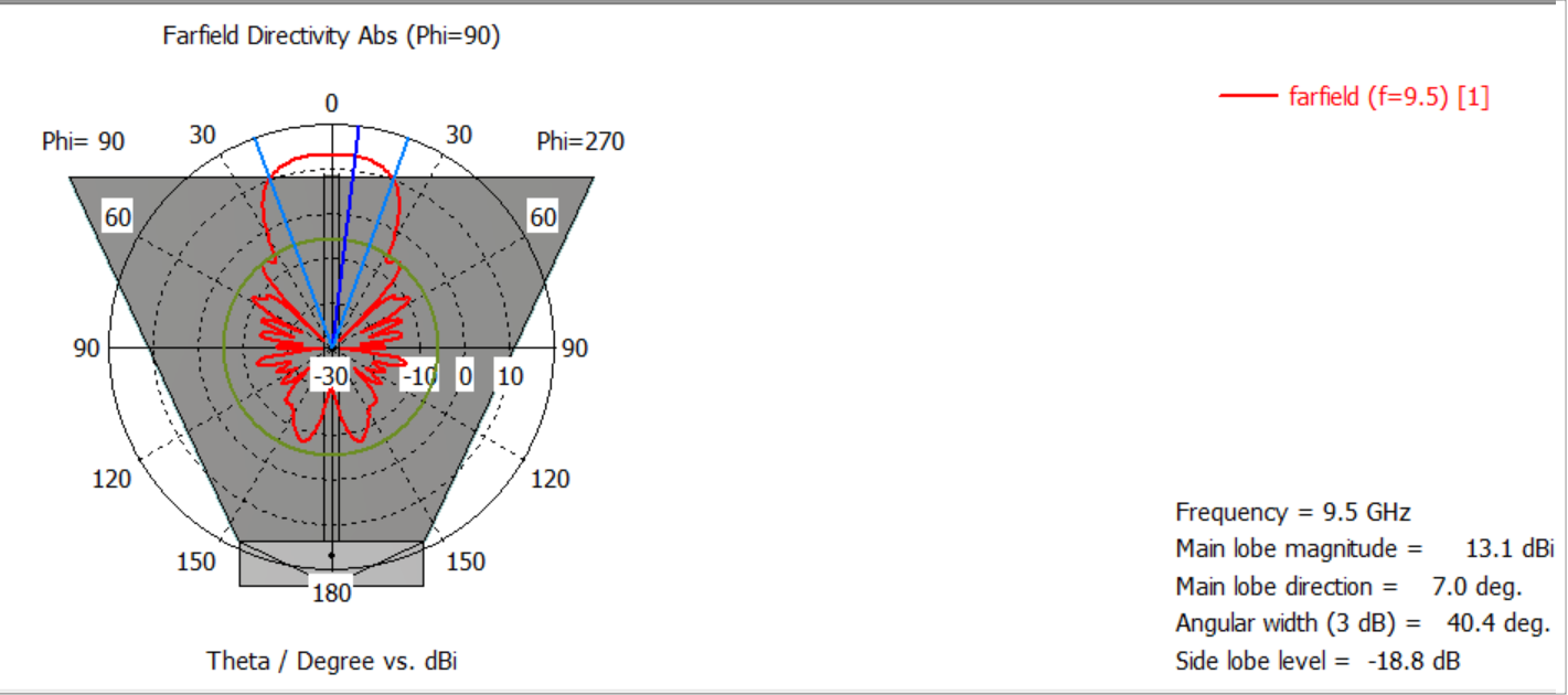
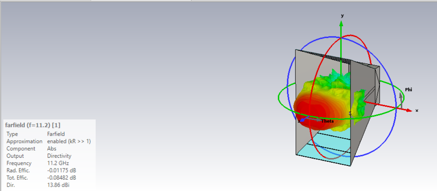
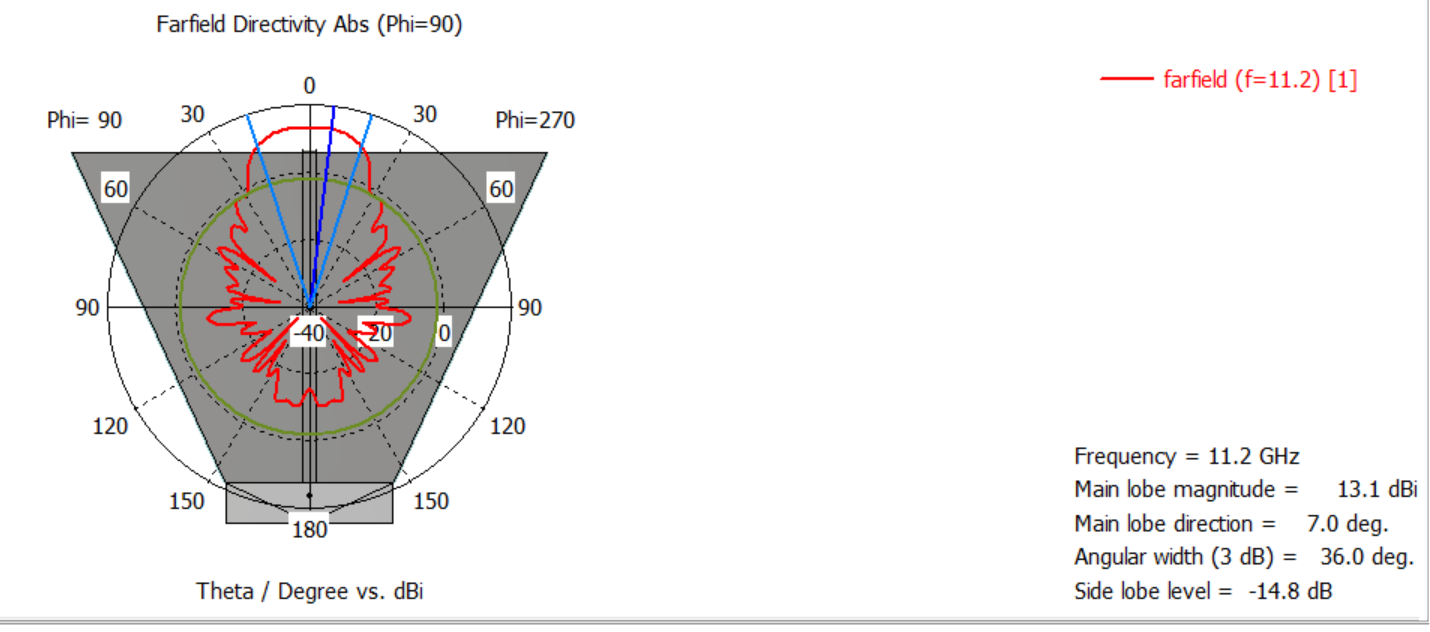
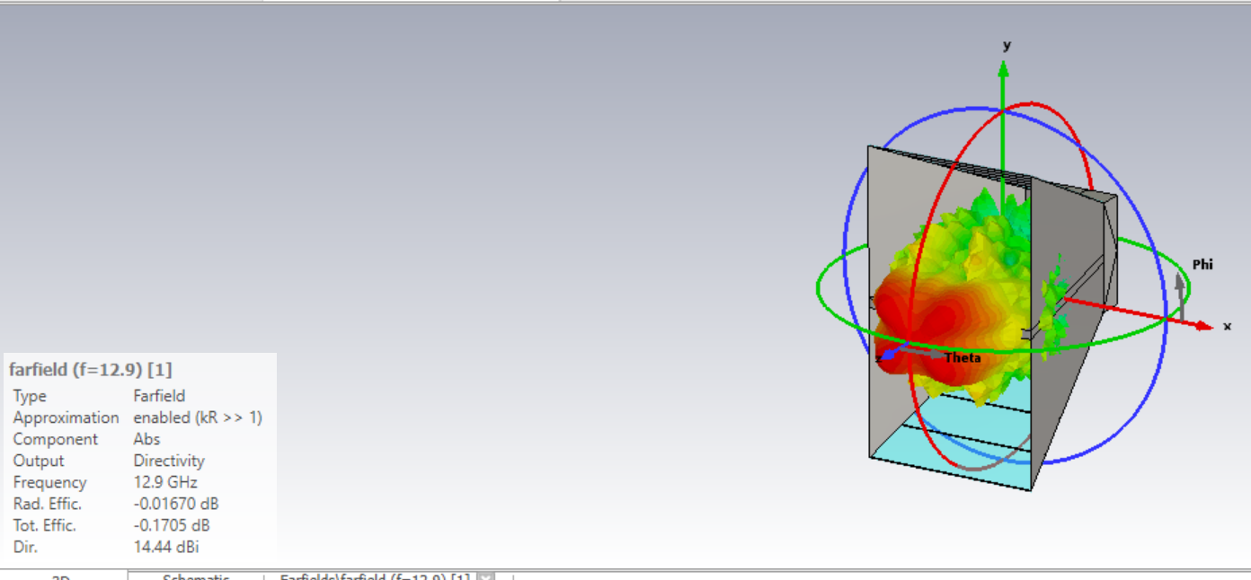
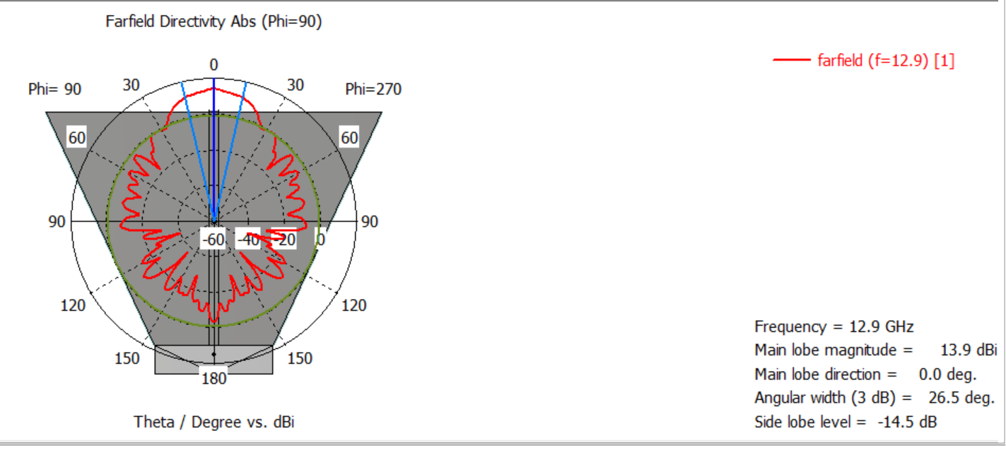
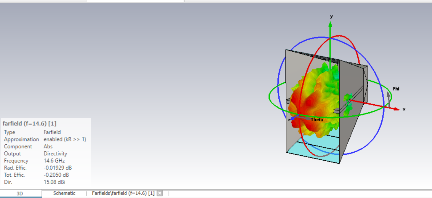
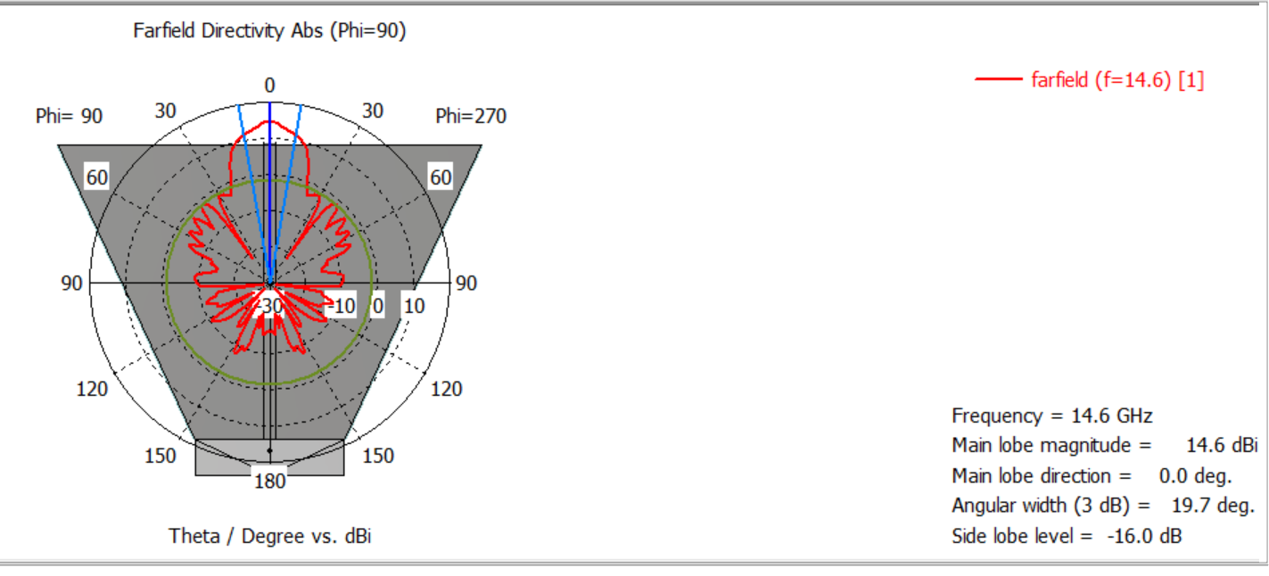
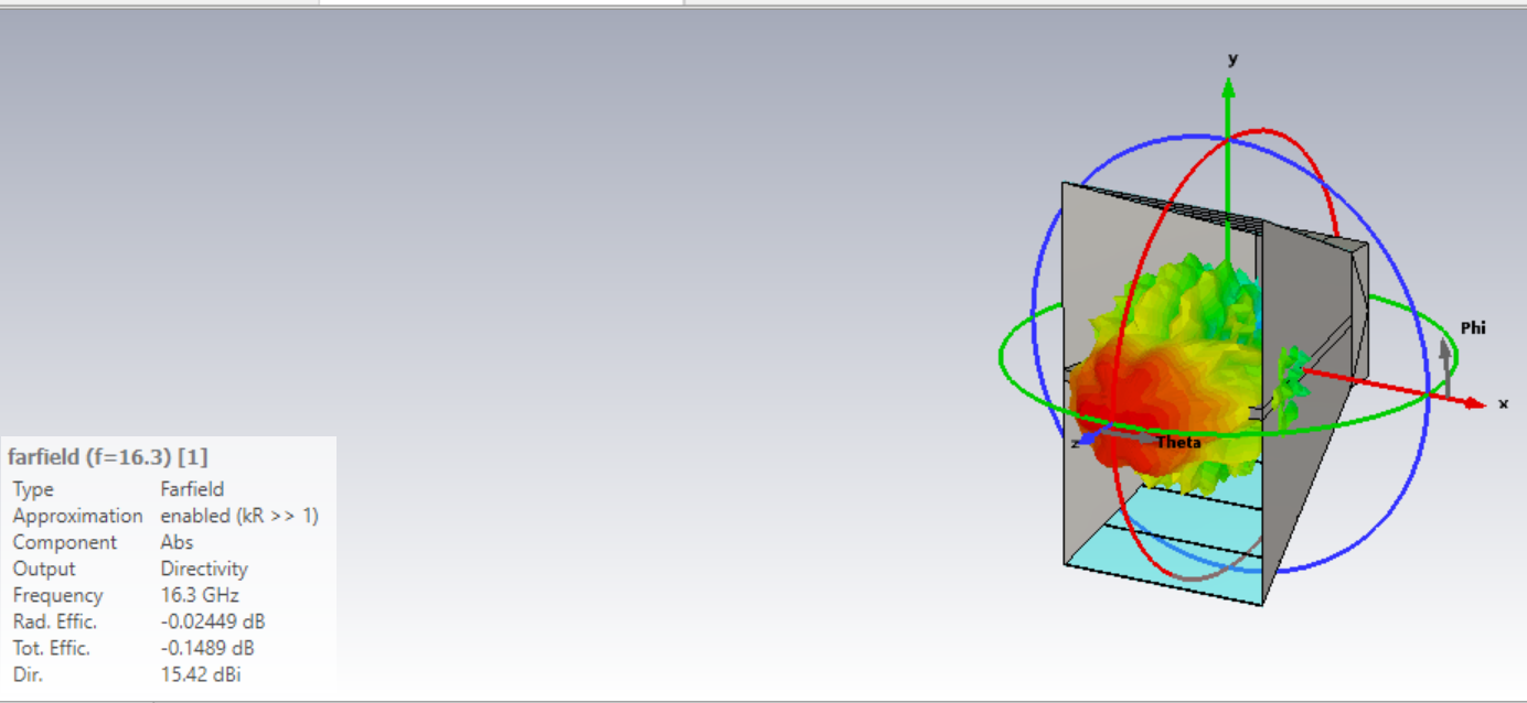
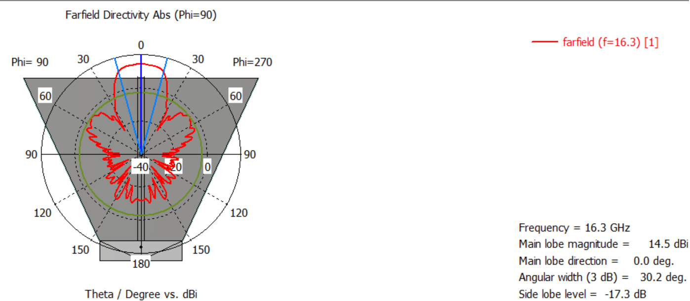
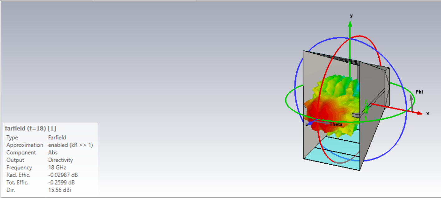
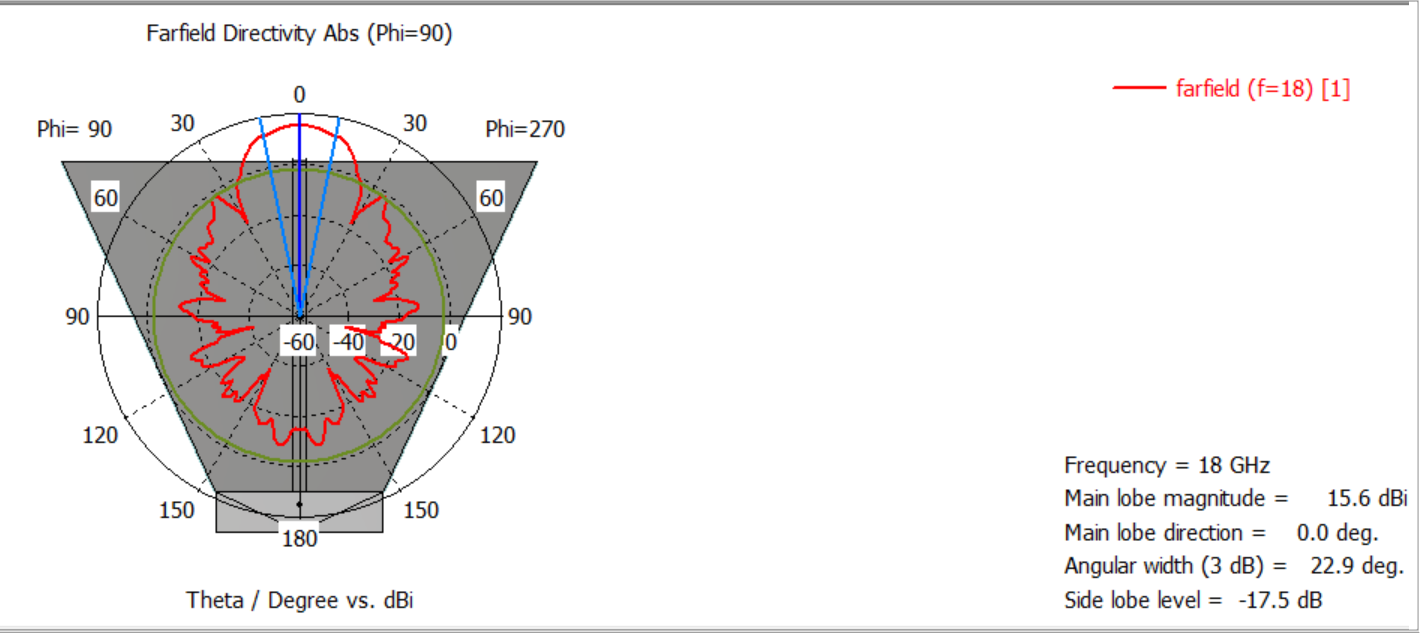
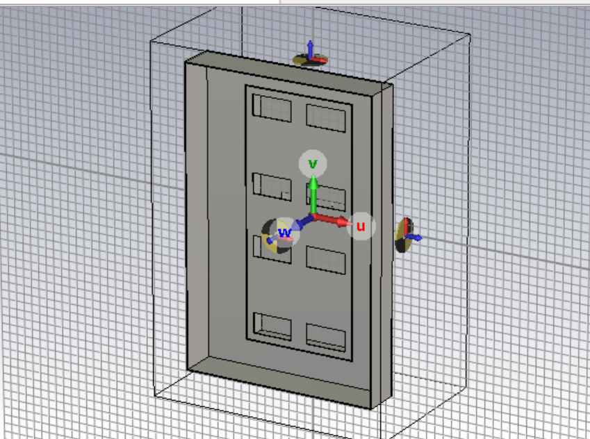
Dual-ridged horn with printed sides for EMC measurements up to 18 GHz
Horn antennas exist in many geometries and are widely used in applications such as electromagnetic sensing, RF heating, biomedical systems, reflector feeds, and as reference antennas for antenna measurements. In several applications—particularly ultra-wideband (UWB) systems and electromagnetic compatibility (EMC) testing—the antenna must maintain stable performance across a very wide frequency range. For measurements covering 1–18 GHz, the double-ridged guide horn (DRGH) is commonly used due to its ability to achieve wide bandwidth with relatively stable radiation patterns.
Historically, achieving this bandwidth while maintaining good impedance matching and radiation pattern stability has been challenging. Many designs reported in literature experienced pattern degradation above approximately 12 GHz, where the radiation pattern splits into four lobes instead of maintaining a single main beam, accompanied by a boresight gain reduction of around 6 dB, as reported by researchers such as Bruns et al. To address this limitation, improved DRGH designs were later developed where both the waveguide launcher and ridge geometry were optimized, achieving a VSWR below 2:1 across an 18:1 bandwidth while maintaining a stable radiation pattern without beam splitting, as demonstrated in work by Jacobs et al.
In the improved architecture proposed in literature, the traditional H-plane metallic walls were removed and replaced by a parallel grid of conducting posts to improve broadband performance. For practical implementation and environmental protection, these conducting posts can be replaced by printed conductive strips on a dielectric substrate, which provides structural support and weatherproofing while maintaining similar electromagnetic behavior.
Building on these principles, a wideband dual-ridged horn antenna with printed sidewalls was designed to operate over the 1–18 GHz frequency range. The dual ridges increase the capacitance inside the waveguide section, effectively lowering the cutoff frequency and enabling broadband operation. The antenna geometry was optimized by carefully tuning key parameters that influence impedance matching and radiation characteristics.
Reducing the ridge spacing lowers the minimum operating frequency but may introduce impedance mismatch at higher frequencies. Increasing the horn flare length generally improves the boresight gain across the band, although excessive flare length may reduce the linearity of the gain response versus frequency. Adjusting the ridge width can improve gain linearity, but larger ridge widths may degrade VSWR performance. Similarly, increasing the bush diameter in the feed region may cause VSWR and gain degradation at the upper frequencies, while using a larger connector pin diameter can improve high-frequency VSWR at the expense of slight gain reduction near frequencies around 16 times the minimum operating frequency.
To maintain stable radiation patterns, the dielectric substrate supporting the printed strips was kept thin and with low relative permittivity, and the printed conductive strips were also designed to be narrow. Increasing substrate thickness or permittivity may disturb the field distribution and lead to radiation pattern splitting in the mid-band region, rather than maintaining a single dominant main lobe.
The final design demonstrates broadband impedance matching, stable radiation patterns, and consistent boresight gain across the 1–18 GHz band, making it suitable for EMC measurements, broadband antenna testing, and wideband RF sensing applications.
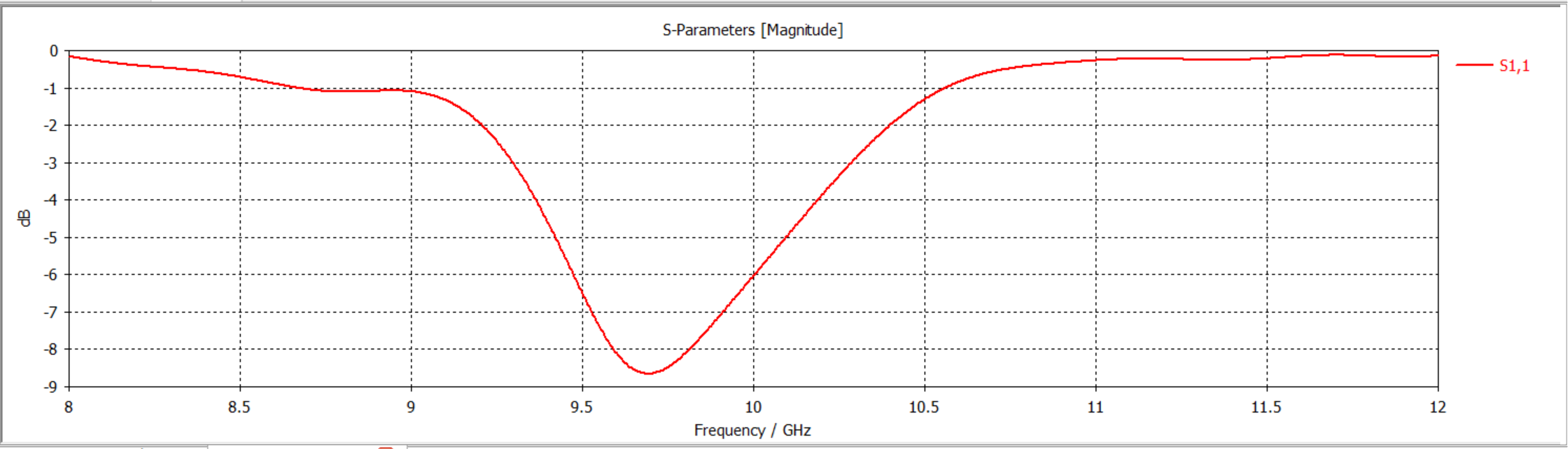
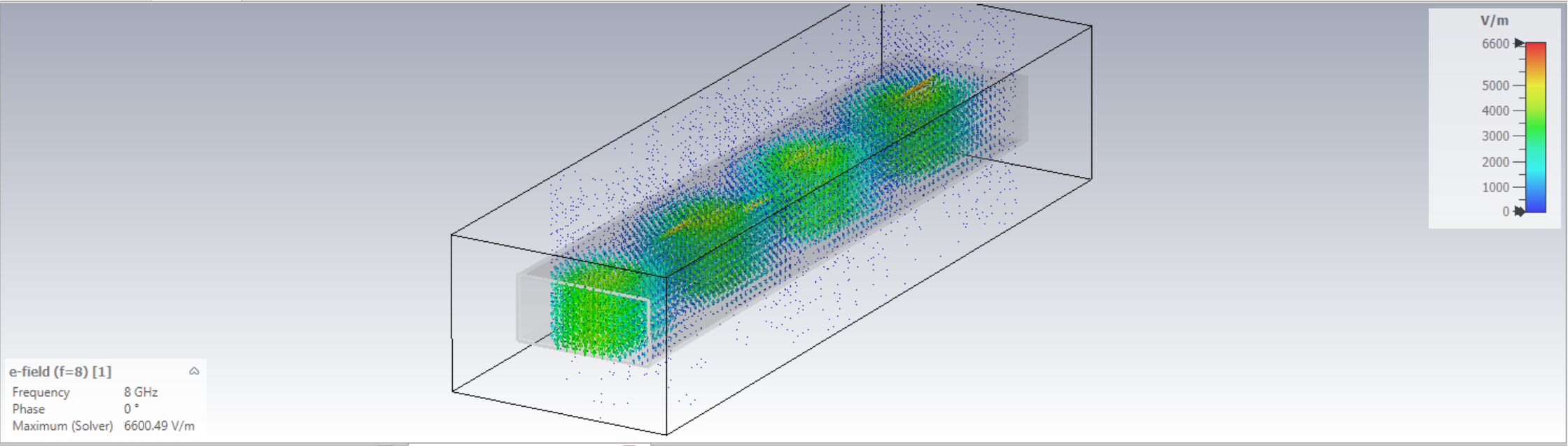
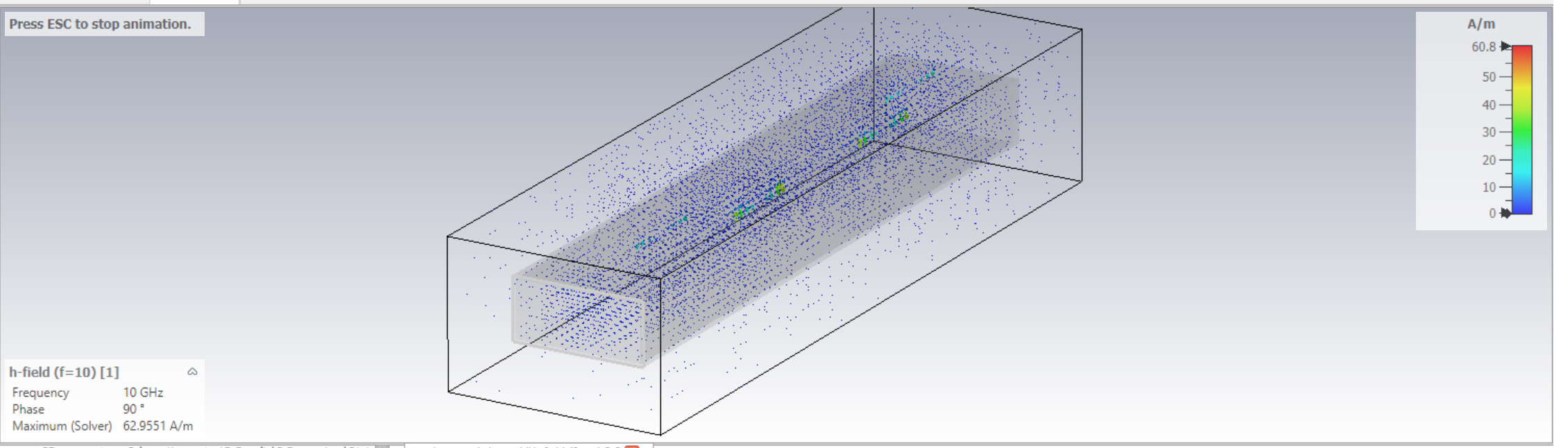
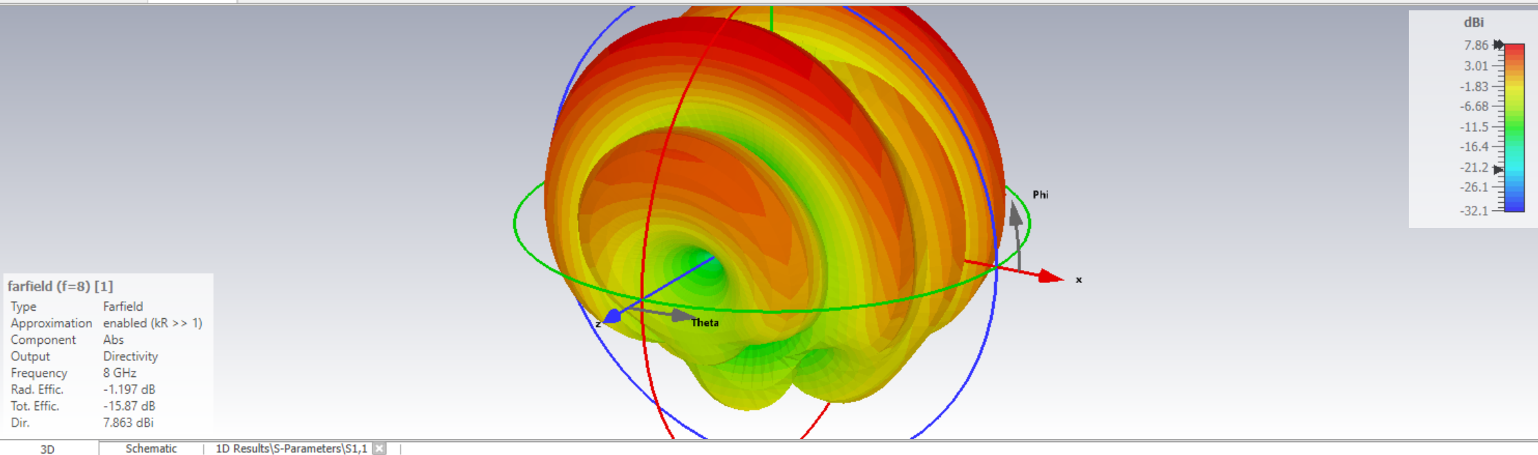
Cavity backed slot antenna array at 30 GHz
A cavity-backed slot antenna array was designed to operate at 30 GHz, targeting millimeter-wave applications that require compact size, high efficiency, and controlled radiation patterns. Slot antennas operate based on the principle that slots cut into a conductive surface act as complementary radiating elements to dipoles, where radiation is produced by the electric fields across the slot aperture.
The proposed design consists of eight rectangular slots arranged at equal spacing within a rectangular metallic cavity structure. The cavity backing serves an important role by suppressing backward radiation, improving front-to-back ratio, and enhancing radiation efficiency. It also stabilizes the radiation pattern and reduces unwanted coupling with surrounding structures.
Each slot is designed to resonate near 30 GHz, where the slot length is typically close to half of the guided wavelength in the structure. The slots are placed at uniform spacing to form a linear array, allowing the radiated fields from individual elements to combine constructively in the broadside direction, resulting in higher gain and improved directivity compared to a single slot antenna.
The cavity-backed configuration also improves impedance matching and bandwidth stability, while the array arrangement enhances the overall aperture size and radiation performance. Such antennas are commonly used in millimeter-wave radar systems, high-frequency communication links, and sensing applications where compact, high-gain planar structures are required.
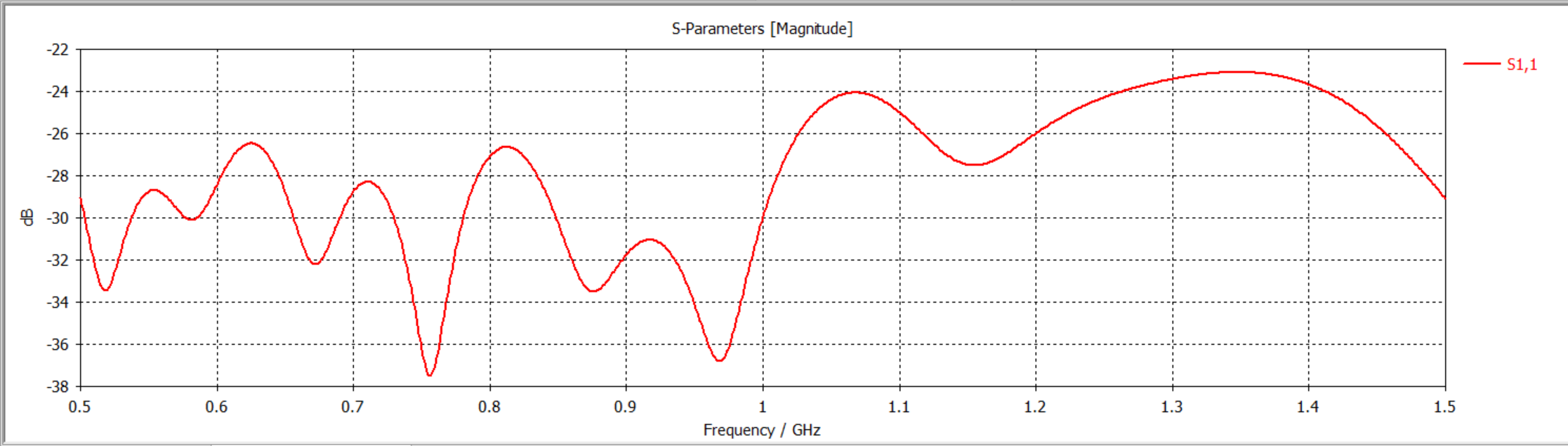
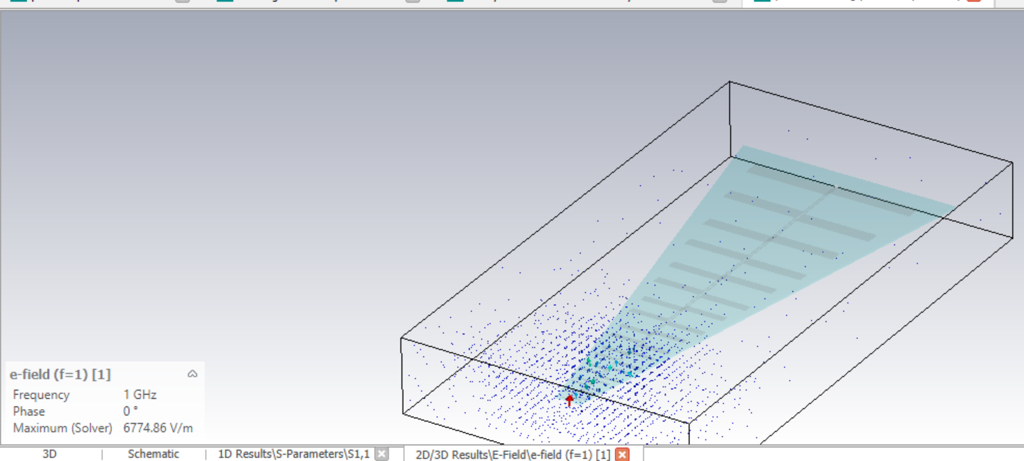
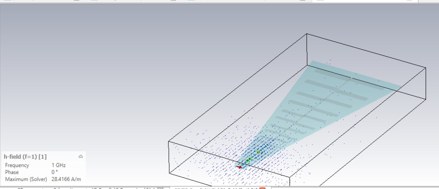
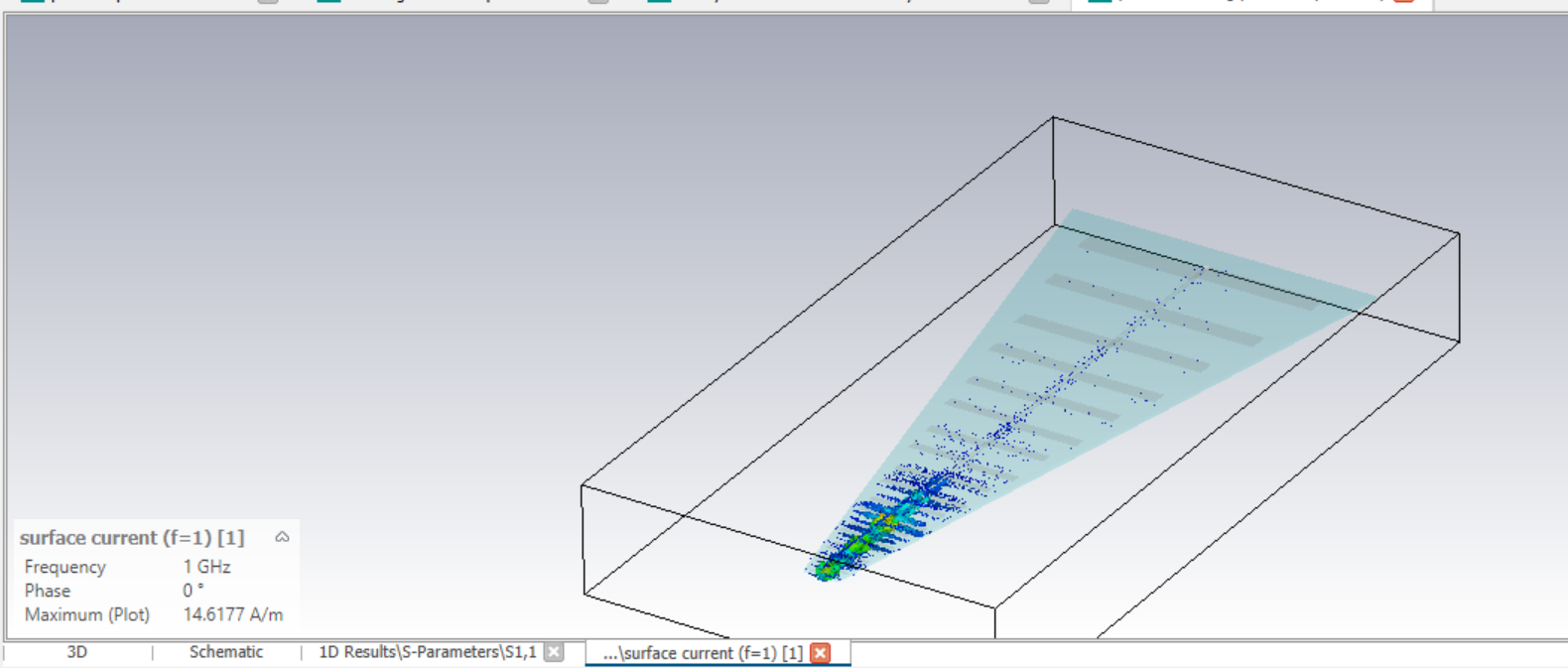
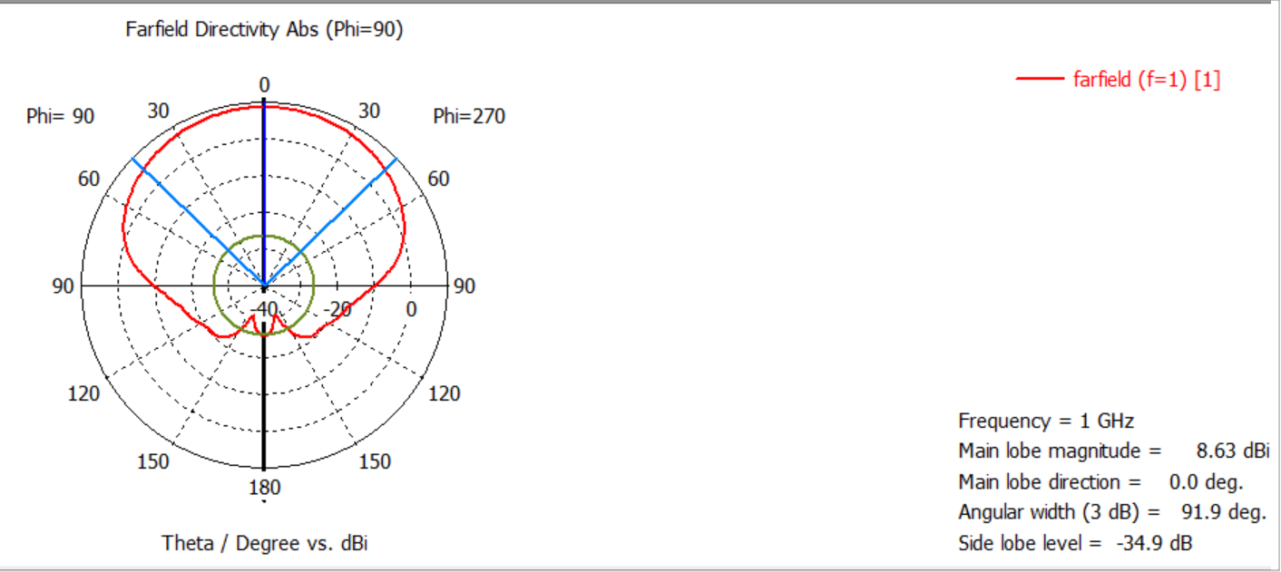
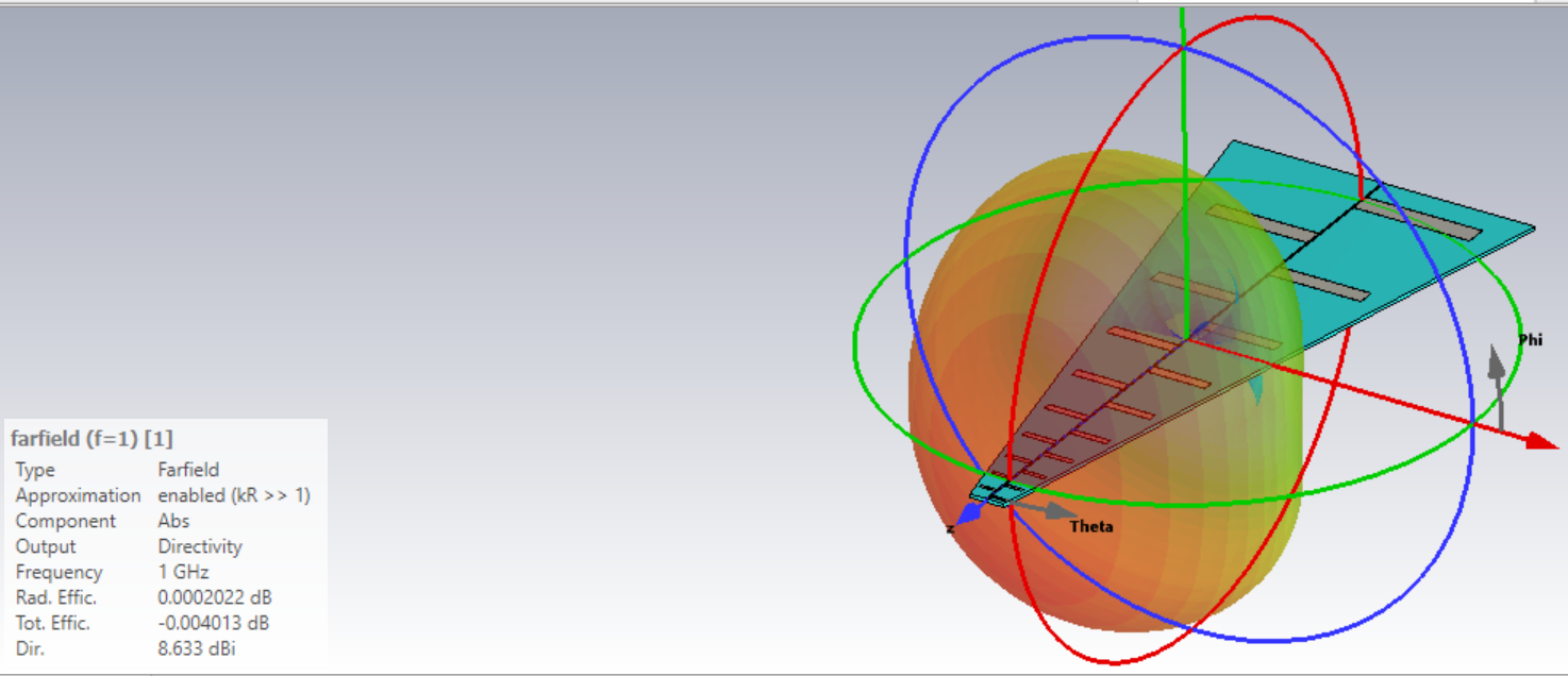
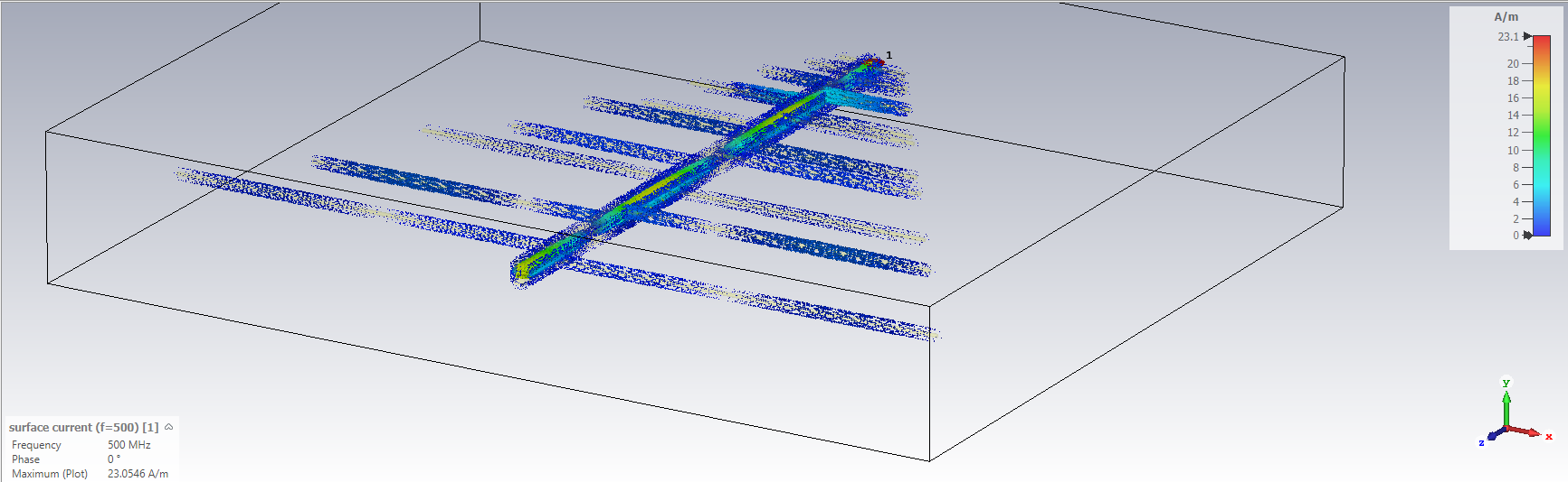
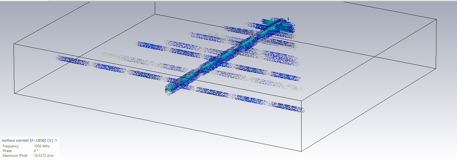
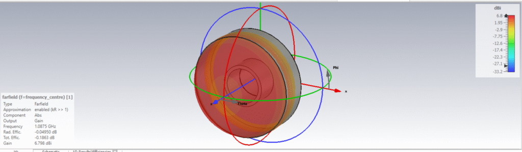
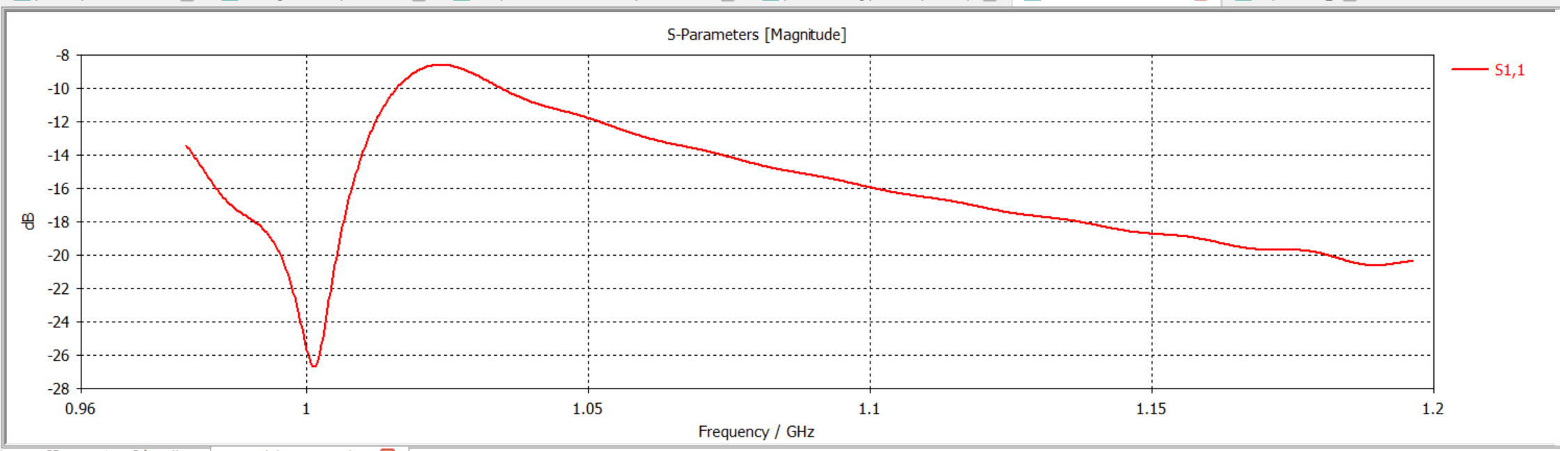
Log-periodic Dipole array at 1 GHz.
5-element slot array with SLL=-7 dB and Gain of 12 dBi.
Slot antennas and dipole antennas are electromagnetic complements. Vertical polarization is crucial for long-distance ground wave propagation. Horizontal dipole = horizontal polarization, and vertical dipole = vertical polarization. But a horizontal slot=vertical polarization.
At 10 GHz, WR90 waveguide is used with specific dimensions. Width=23.85 mm and Height (b)=10.16 mm. Fc=6.56 GHz, The slots can be cut:
Fc can be calculated. The modes with f > fc will propagate; modes with f < fc will be in cutoff or evanescent mode.
Coaxial cavity Horn Antenna
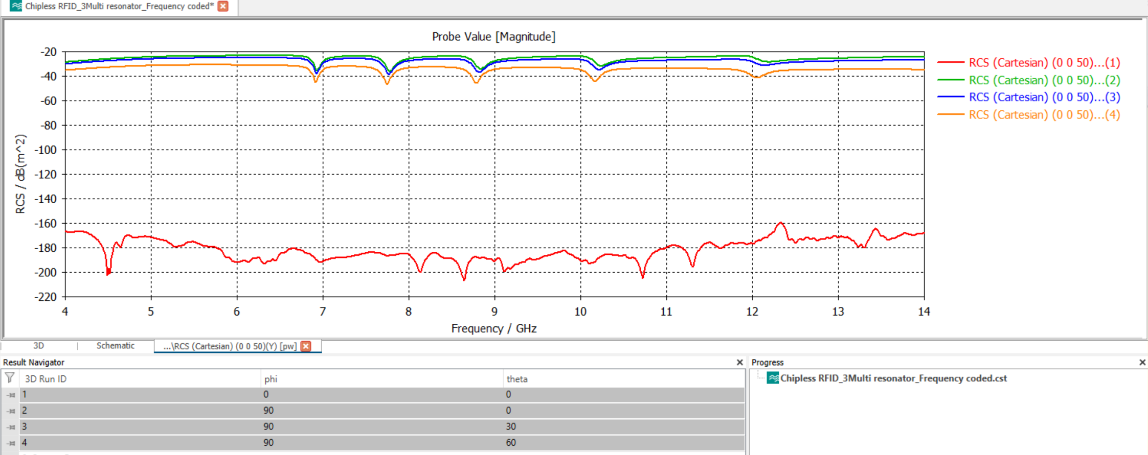
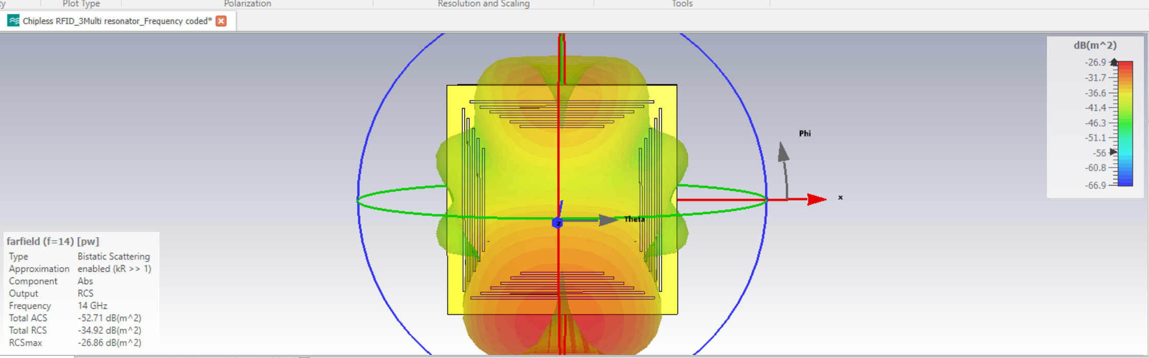
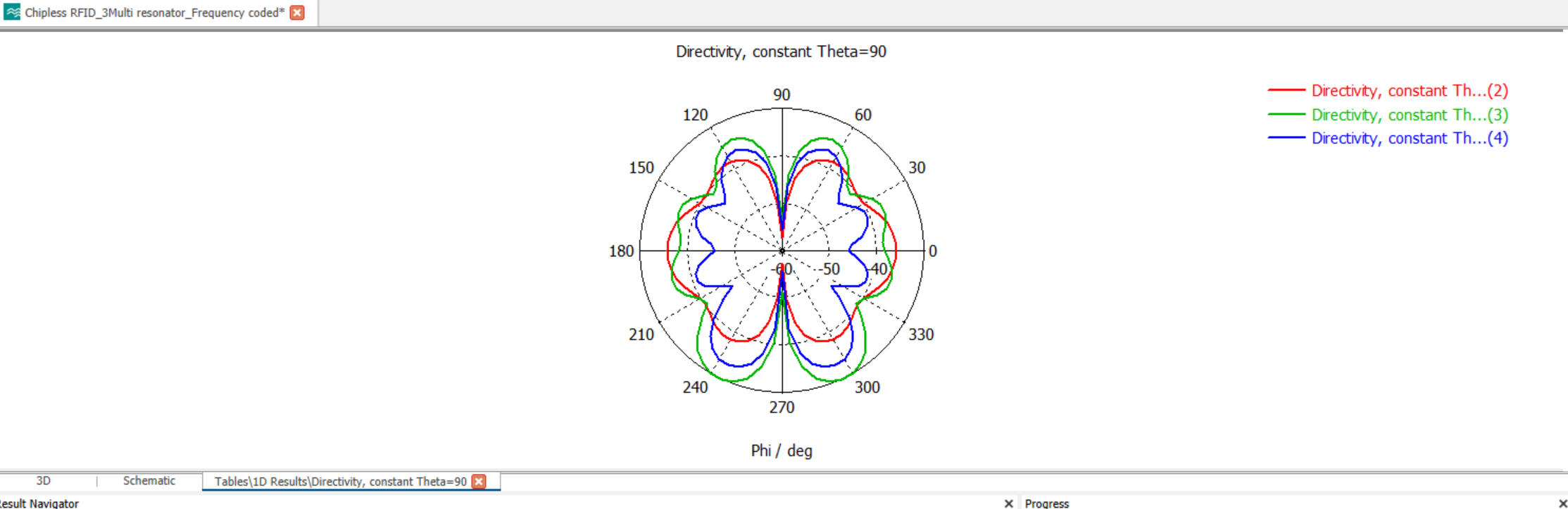
Chipless RFID tags Simulations in CST Stuudio Suite.
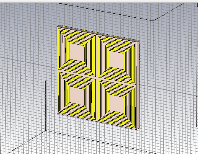
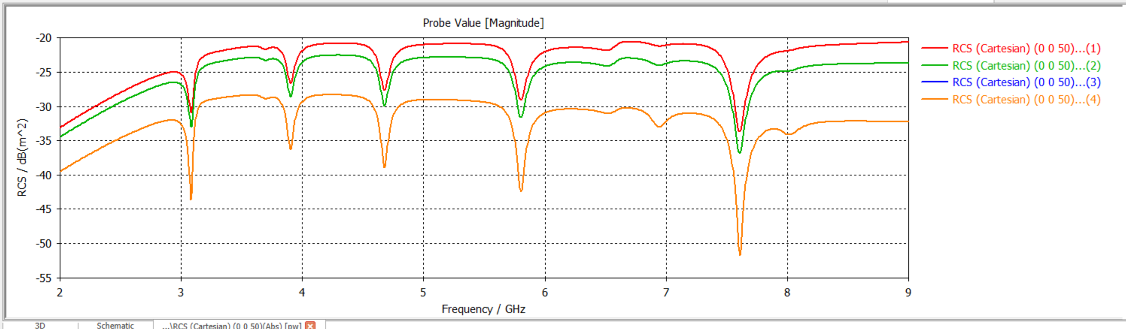
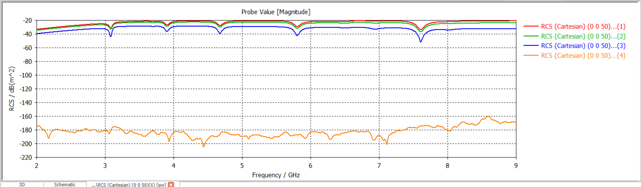
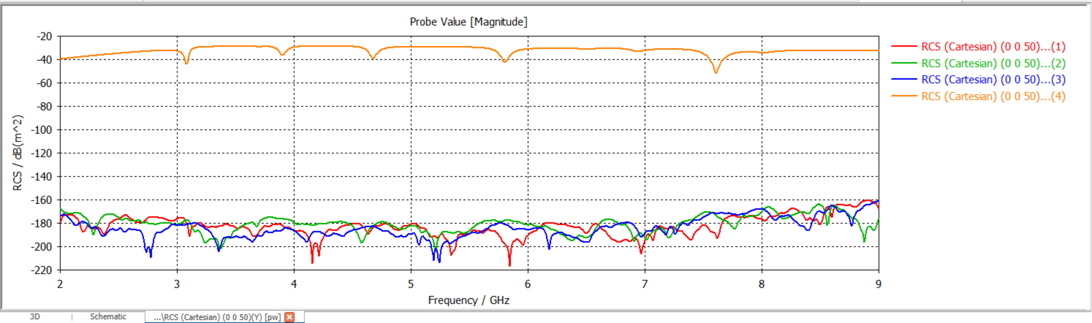
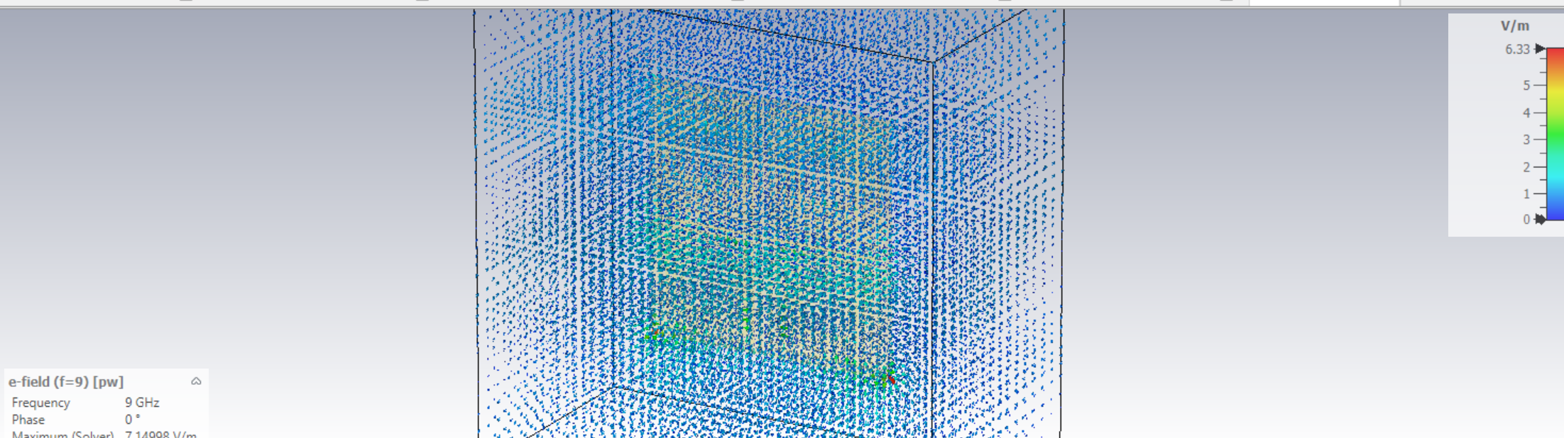
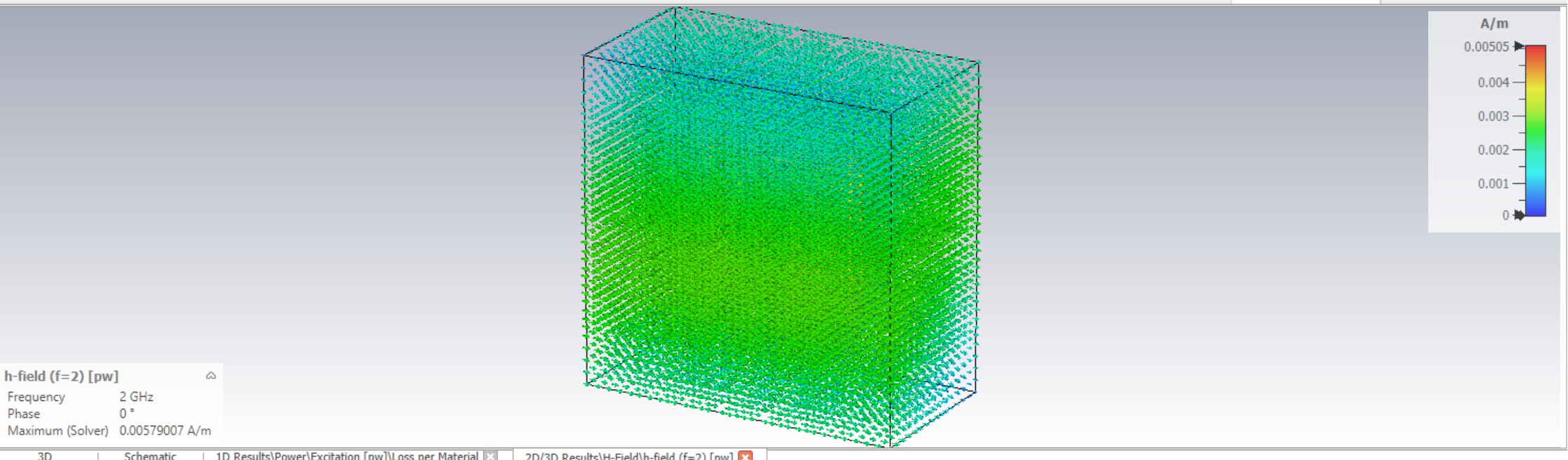
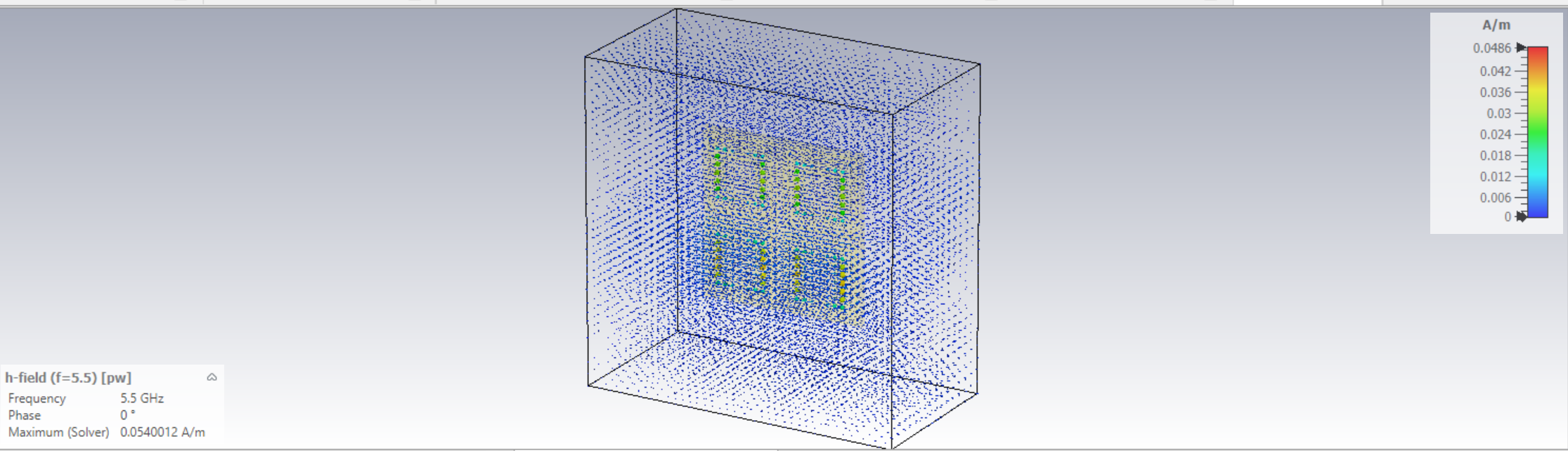
Chip-less RFID tag design from 2-9 GHz resonances.
RFID uses EM waves to identify and track tags attached to objects. Each tag contains electronically stored information, readable by a nearby RFID reader.
Components of RFID tags: Tag (Transponder): Contains antenna and chip/memory.
Reader (interrogator): Sends an RF signal, powers passive tags, and reads a backscatter signal.
Middleware/Backend: Data filtering, database interaction and system management.
RFID Frequency bands: LF (125-134 KHz): Animal tagging, short range, slow data; HF (13.56 MHz): Smart cards, NFC; UHF (860-960 MHz) Supply chain retail, longer reading range. Microwaves (2.45 GHz): Toll systems, fast reads, sensitive to water / metal.
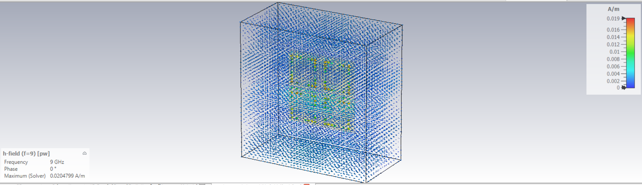
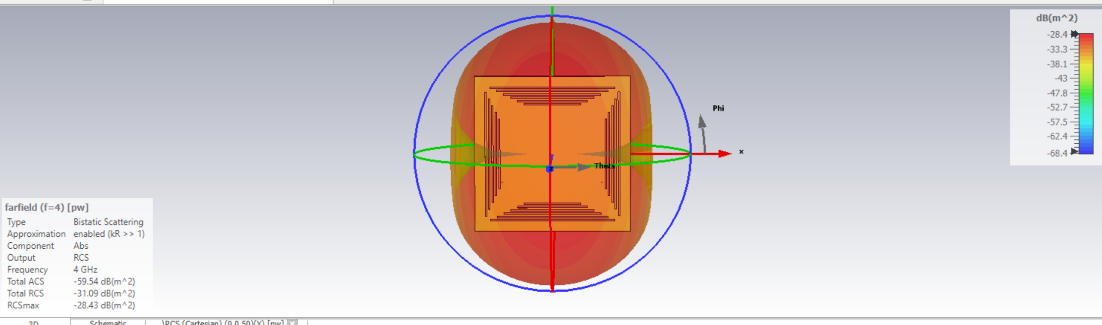
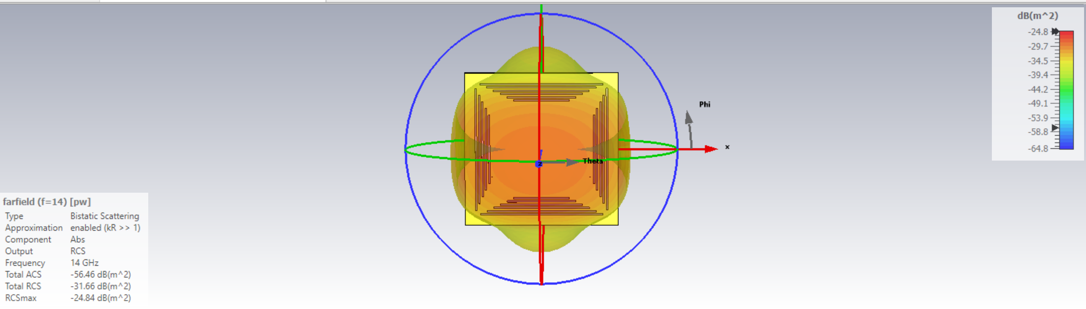
Unit cell size = 30*30 mm². FR4 with 1.6 mm thickness. The nested rings are 0.468 mm wide. and are separated by a gap of the same size. The structure is a metallic frequency-selective surface over a thin grounded dielectric slab.
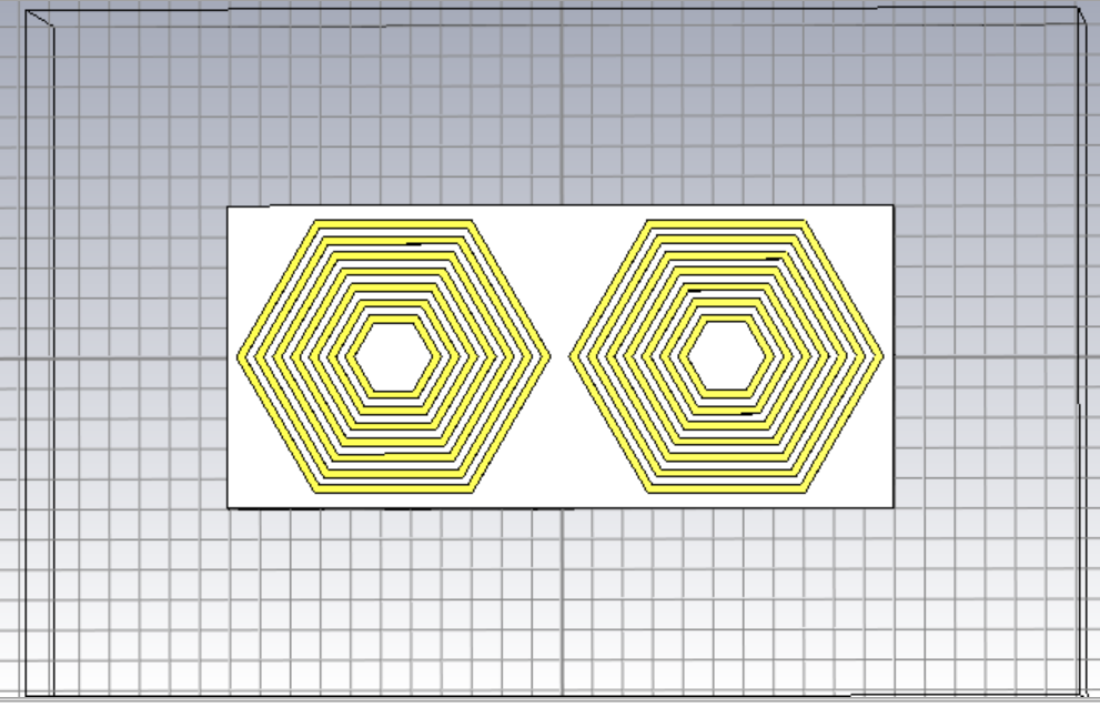
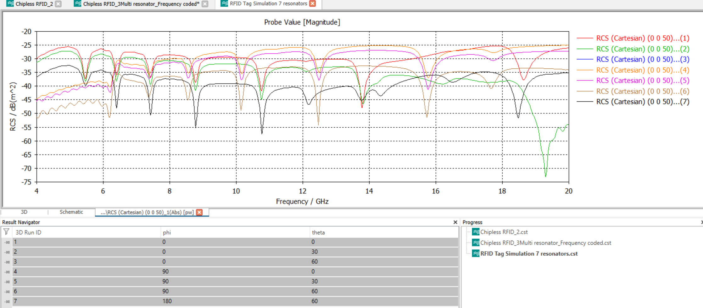
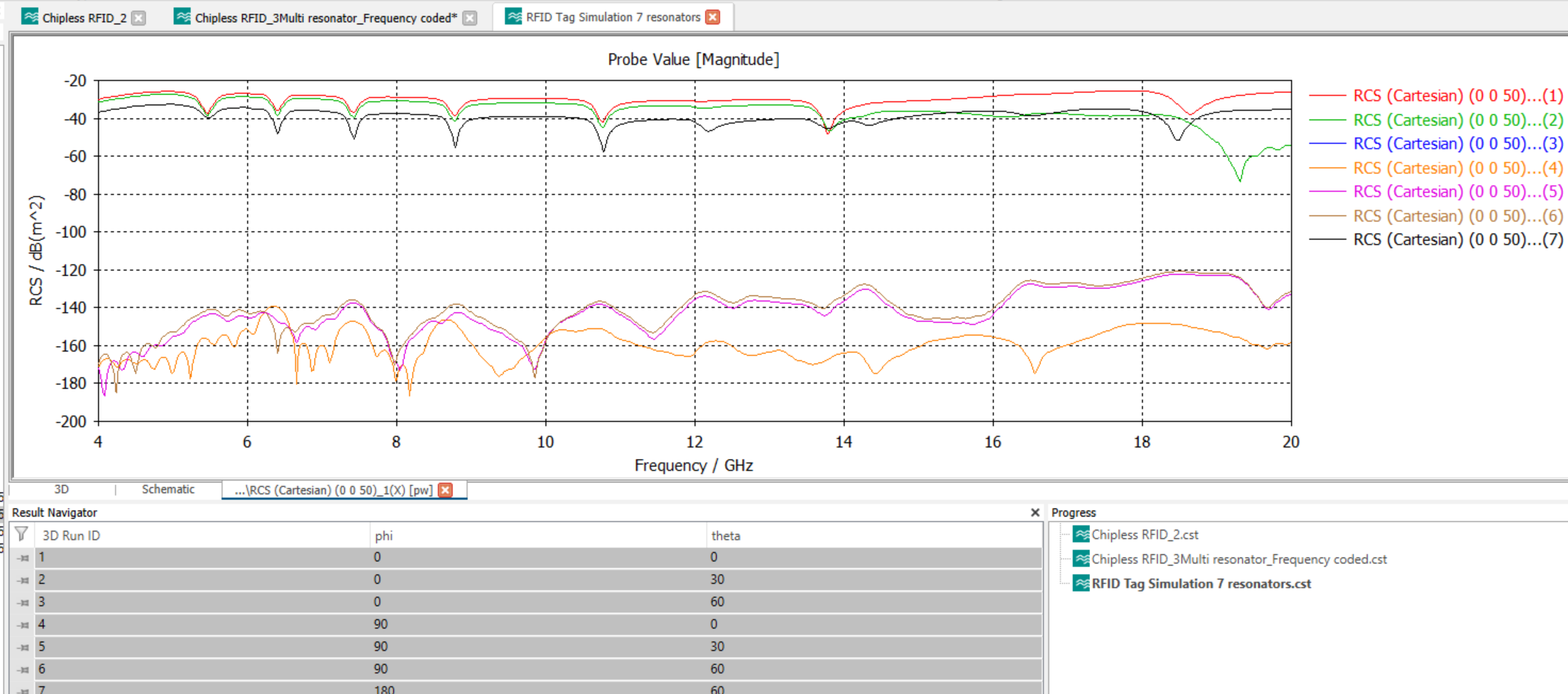
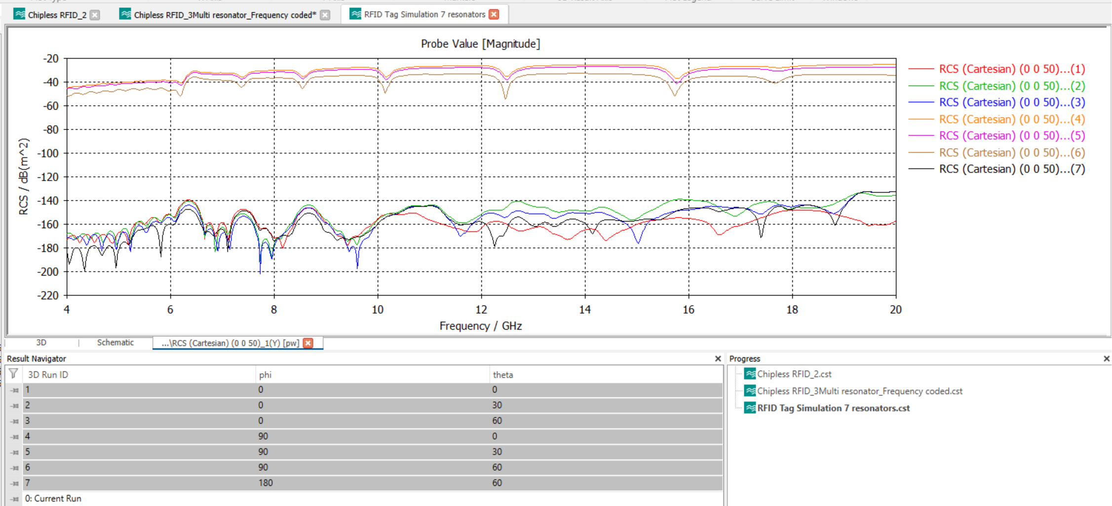
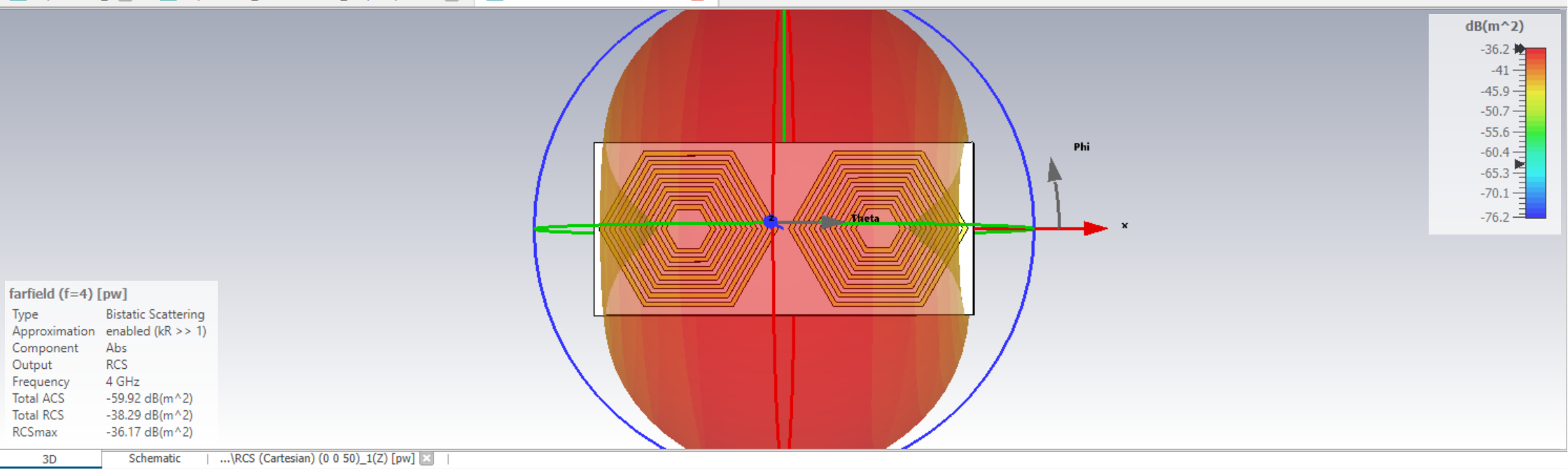
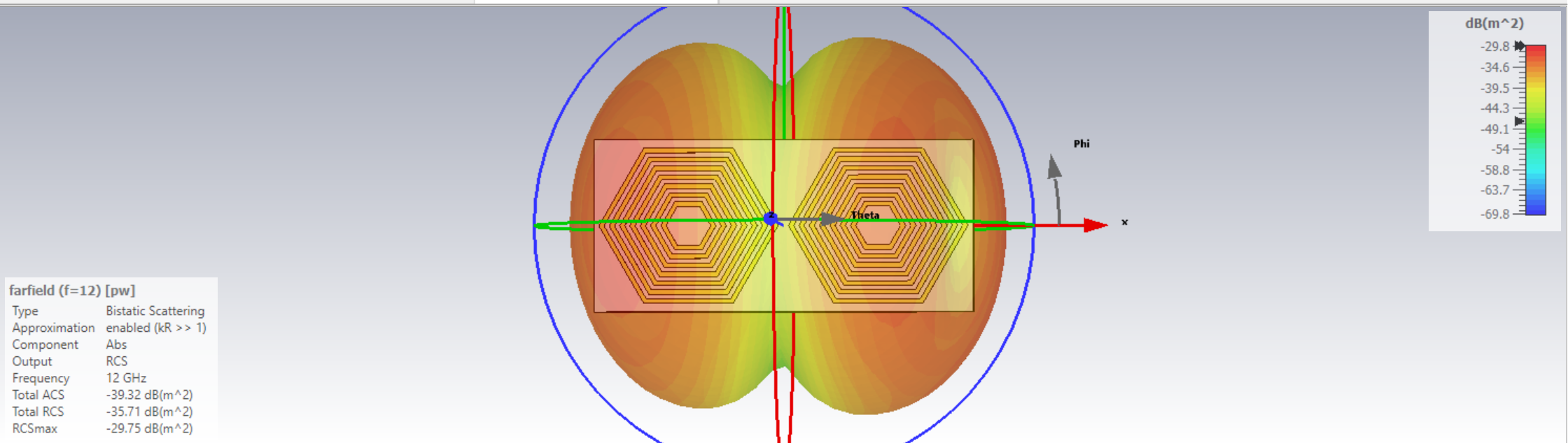
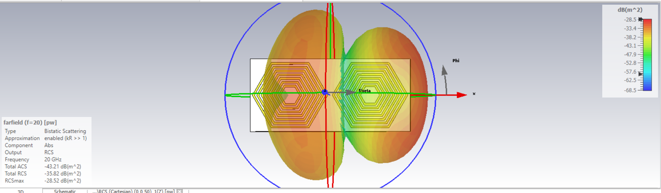
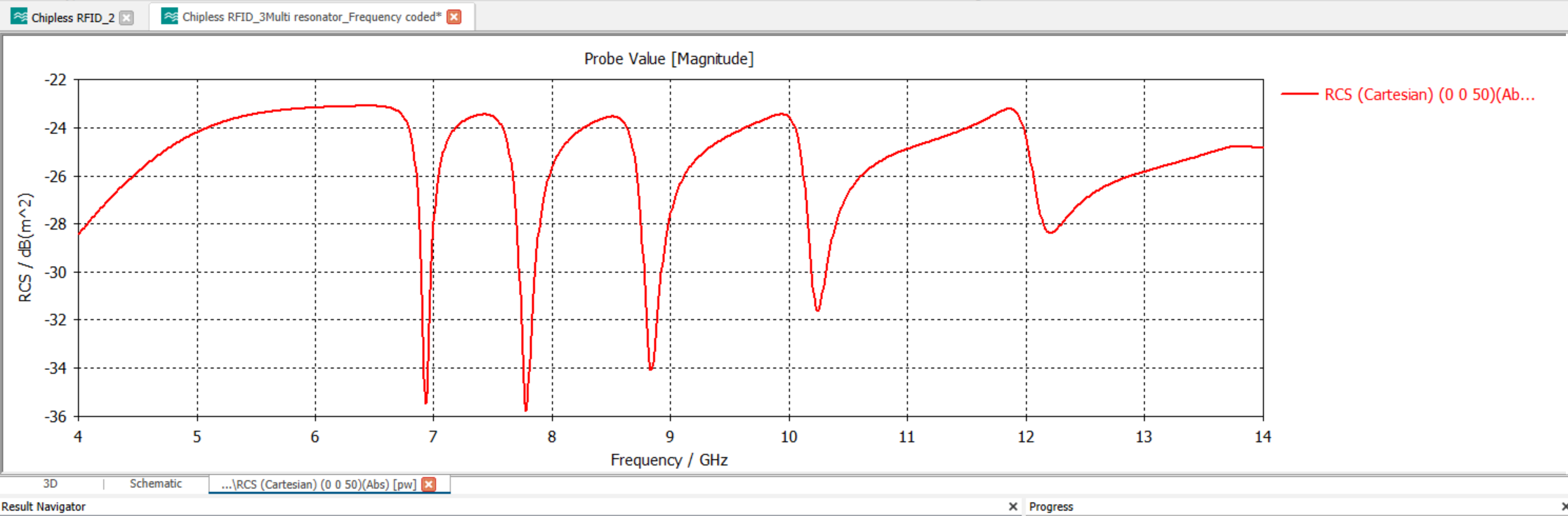
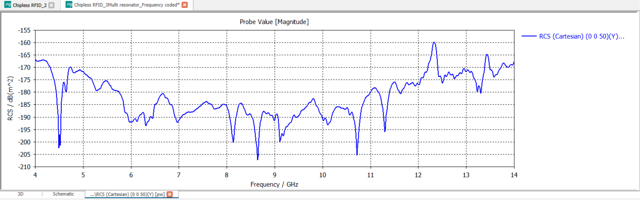
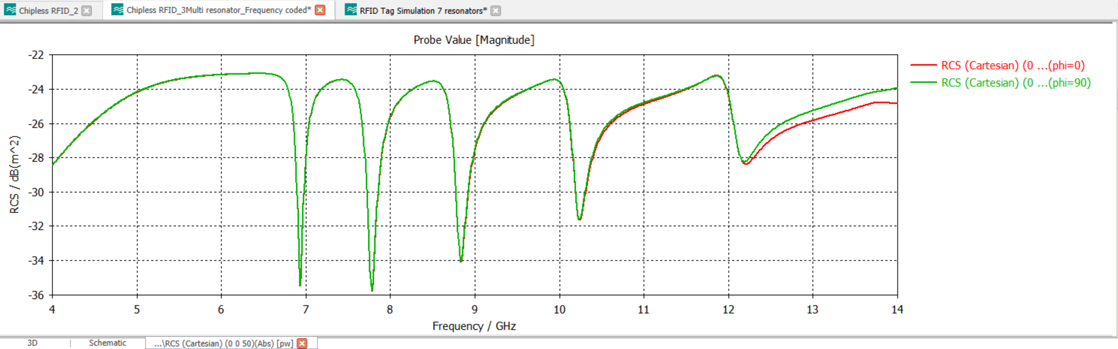
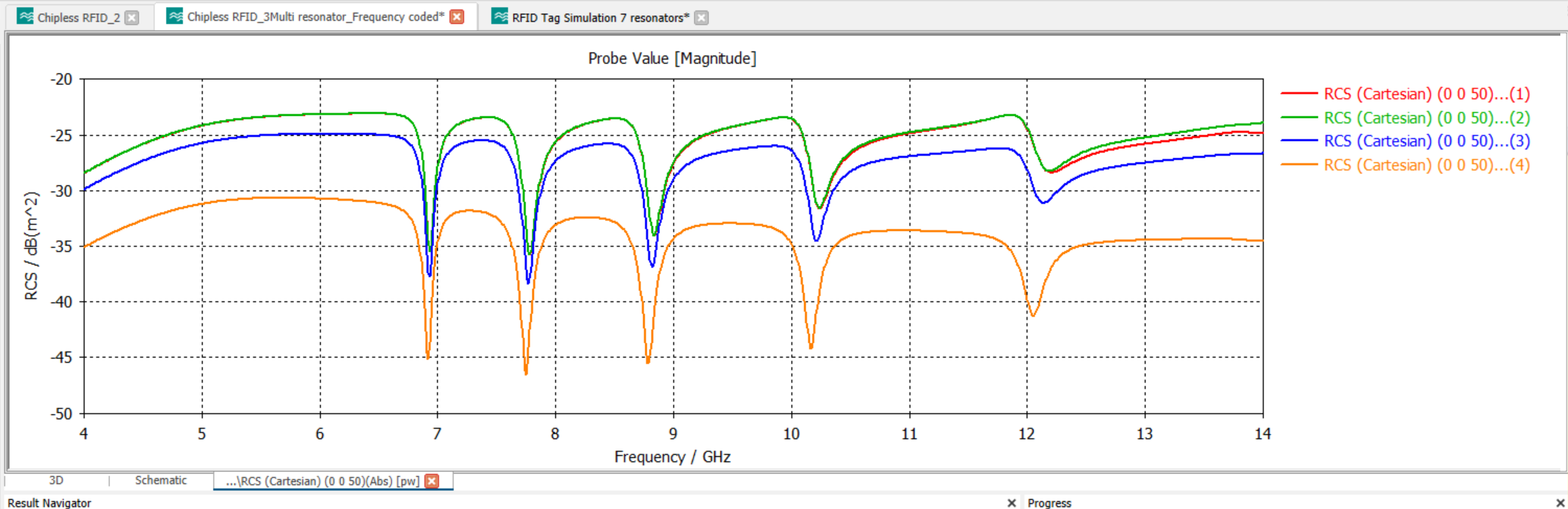
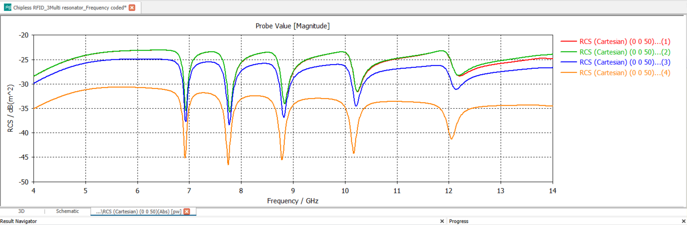
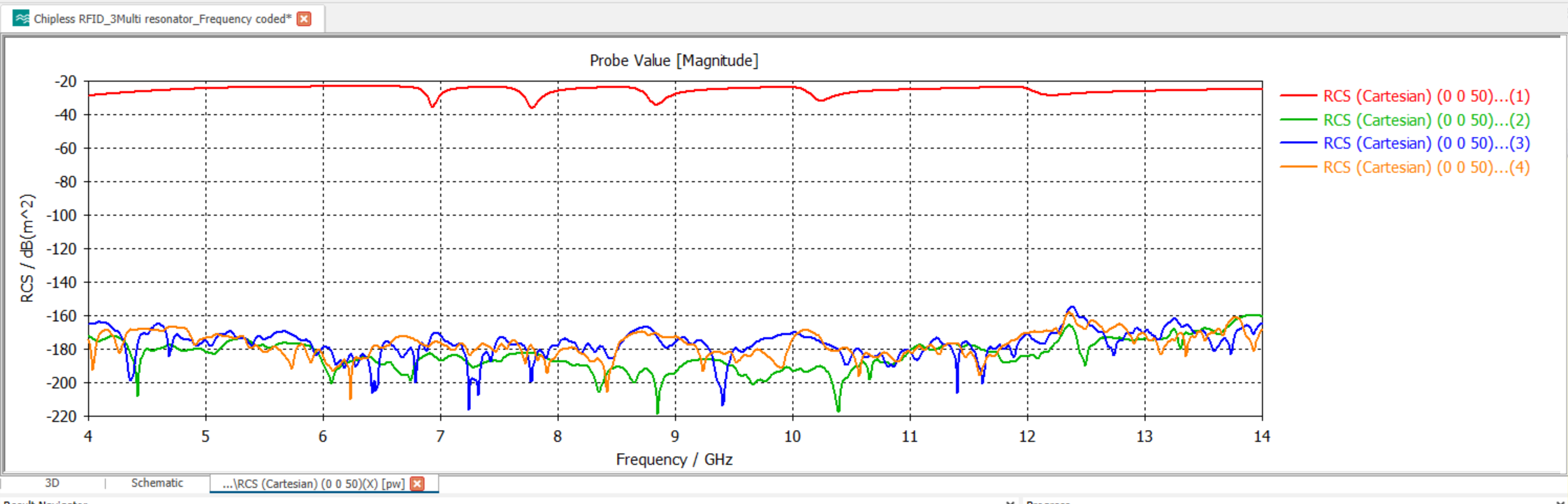
Chipless RFID tag from 4-20 GHz.
Tags that don’t use an integrated chip instead rely on physical or electromagnetic characteristics (like resonators or scatterers) to encode data.
Advantages: ultra-low cost, printable on paper/plastic, suitable for disposable and large-scale sensing.
Applications: Smart packaging, humidity/temperature sensing, document tagging.
Frequency bit mapping: Example, 7 resonators = a 7-bit tag. Frequency spacing must avoid overlap (non-interfering). A notch at 4 GHz = 1, absence = 0.
Ring 1
The substrate used is FR4, 1.6 mm in thickness. The tag consists of a metallic (copper) ground plane. Hexagonal resonators are at the top of the substrate. The spacing between the resonators and the width of the resonators = w = 0.3 mm.
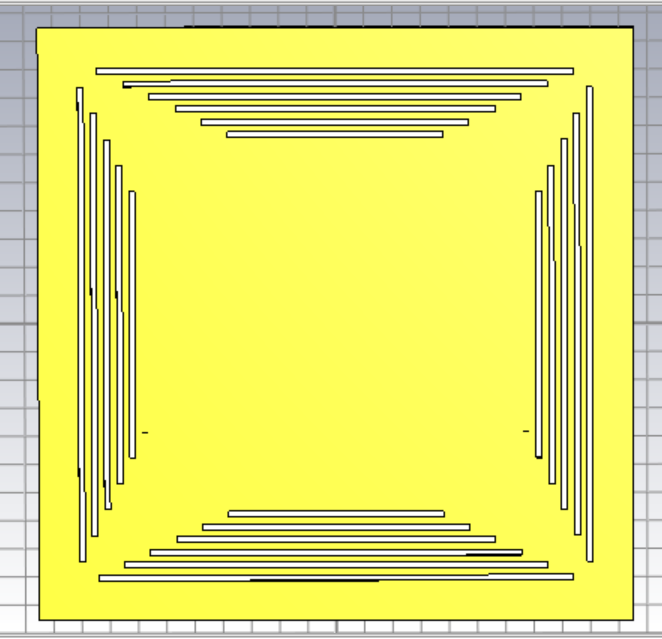
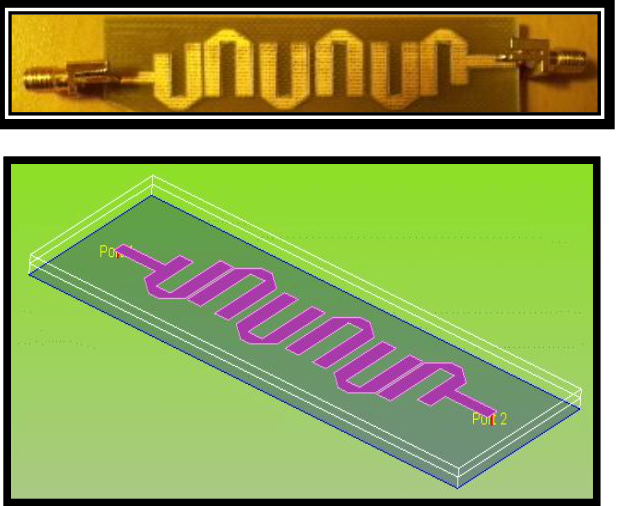
A compact dual-polarised chipless RFID tag using slot length variation in I slot resonators.
First, the “I”-shaped slot resonators are etched from a sqaure metallic patch in both vertical and horizontal directions, which doubles the encoding capacity within a fixed frequency band.
Substrate = Taconiuc TLX-8, substrate thickness = 0.5mm, unit cell size = 21*21 mm²
RF Power Amplifier Design
Being Updated Soon
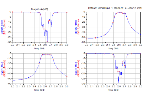
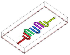
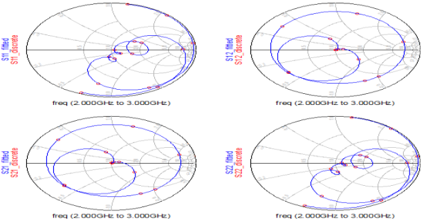
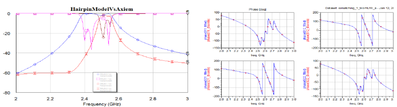
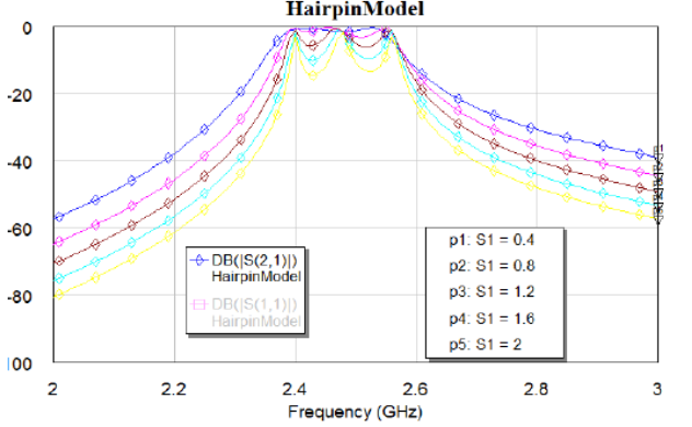
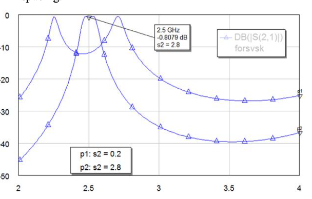
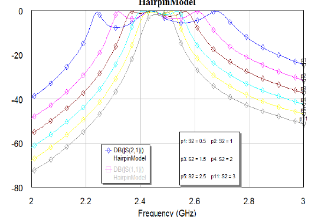
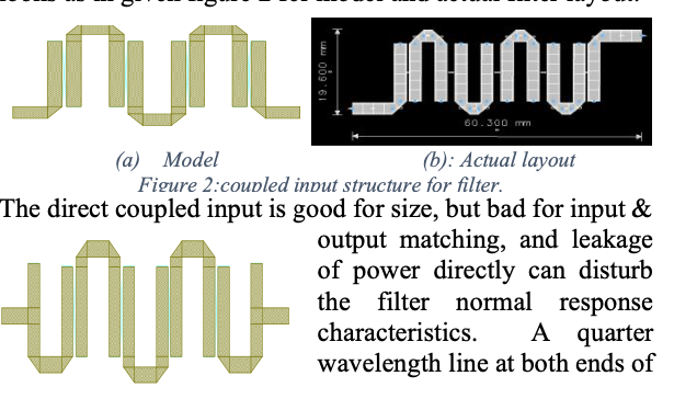
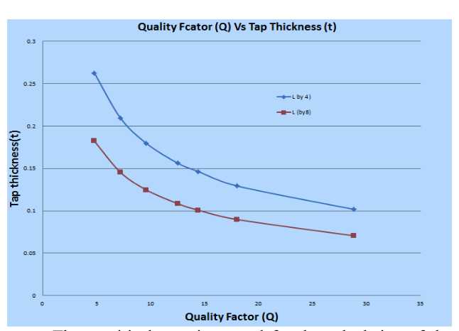
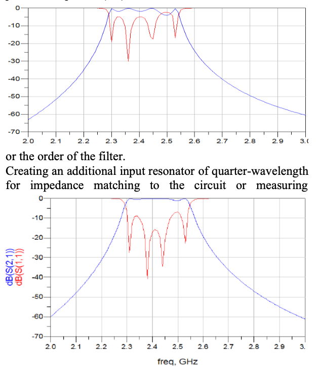
Design and Size reduction analysis of microstrip hairpin bandpass filters.
Abstract—This paper presents the microstrip filter hairpin structure design and analysis in synthesis form. All the elements that can affect the design of hairpin filters are studied using simulations. Some filters are designed and input types (tapped & coupled), are analyzed, the coupling effects & the inter-resonator spacing dependance are studied as well as the spacing effects on the bandwidth. Important design matrix and considerations for narrow and wideband filters are presented with simulation & experimental results.
Keywords—hairpin filters, inter-resonator spacings, coupling coefficient’s.
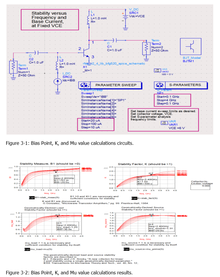
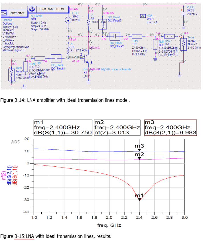
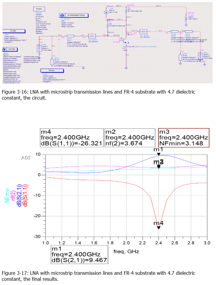
RF LNA Design: Wideband Low Noise Amplifier (LNA) Design at 2.4 GHz Center Frequency.
The design of 2.4 GHz amplifier is demonstrated in this project. The design achieved a gain of approximately 10 dB and noise figure of 3 dB. The Noise figure has the potential to improve but it turns out to be tradeoff as the gain is sacrificed with lower noise figures and the noise figure is increased for modest gains. The transistor used itself presented a relatively modest gain, I.e. maximum stable gain of the amplifier comes out to be 13 dB only. Hence, the selection of active device with inherently low noise figure and reasonable gain needs to be considered as the main target.
In conclusion, the design and implementation of a low noise amplifier (LNA) using the BFG520 transistor in the Advanced Design System (ADS) software have demonstrated successful results. The BFG520 transistor, a high-frequency NPN bipolar junction transistor (BJT), proved to be an excellent choice for the LNA design at the desired frequency range.
Through careful analysis and optimization, the LNA achieved a desirable combination of high gain, low noise figure, stability, and linearity at the designated frequency of operation. The performance of the LNA was characterized by simulating key parameters such as S-parameters, gain, noise figure, stability circles, and input/output matching.
The design process involved various steps, including component selection, biasing, impedance matching, and stability analysis. The BFG520 transistor, known for its low noise characteristics and suitability for high-frequency applications, played a crucial role in achieving the desired performance goals.
By incorporating input and output matching networks, the LNA successfully mitigated impedance mismatches and minimized signal reflections, resulting in improved gain and noise figure performance. Additionally, stability analysis was conducted to ensure the LNA remained stable across the operating frequency range.