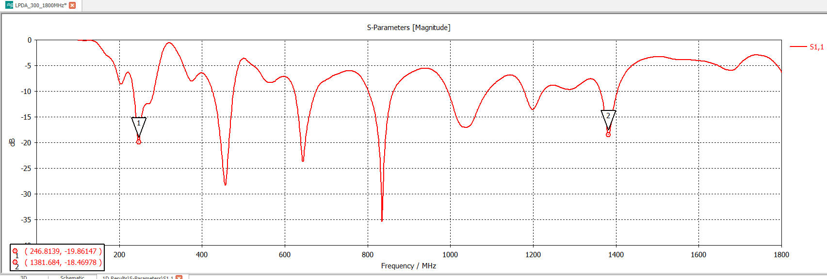
Log-Periodic Dipole Array (LPDA) at VHF (300-1300 MHz) – CST Design | Results & Working Principle
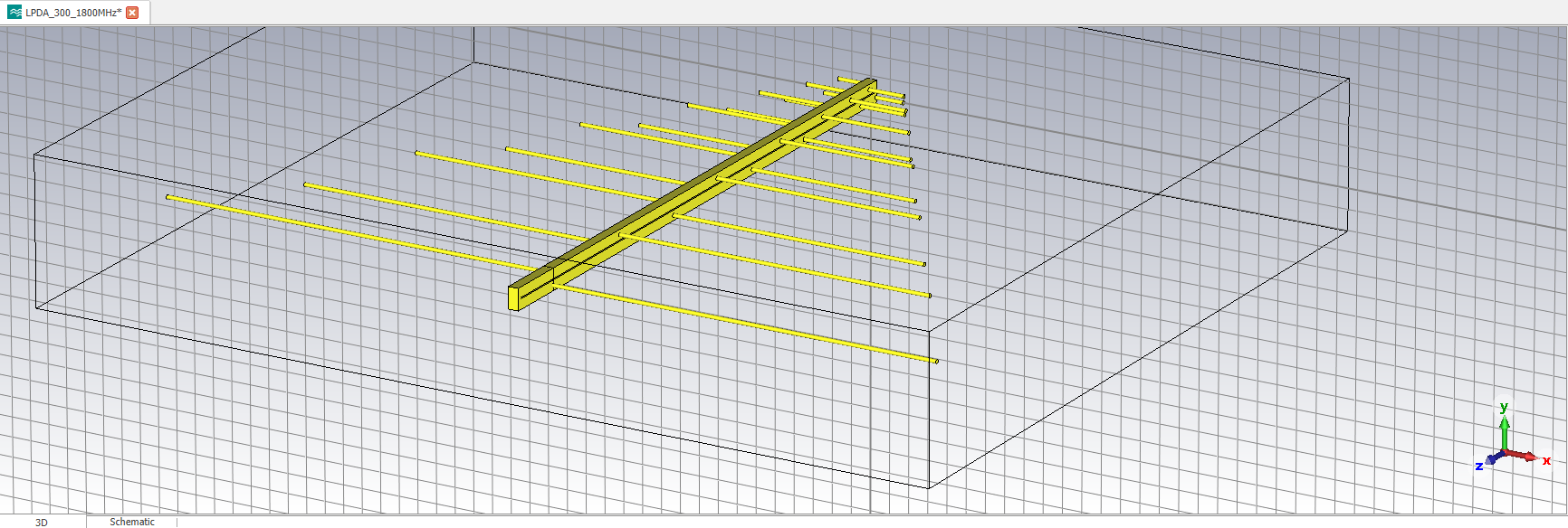
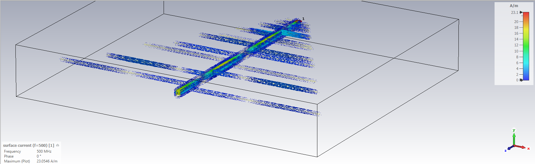
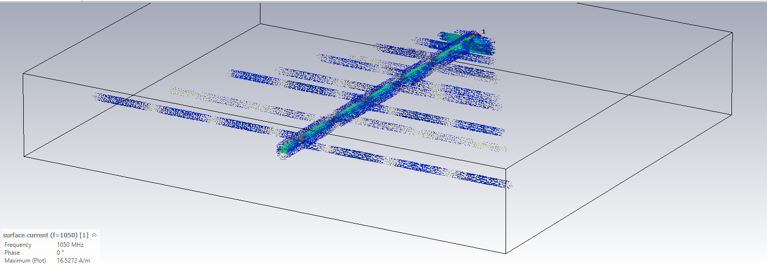
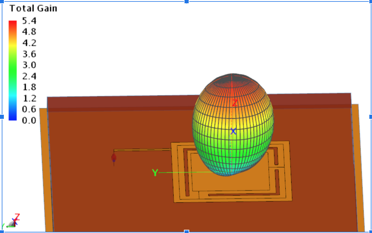
The LPDA consists of multiple dipole elements that progressively decrease in length toward the front, which is the direction of maximum radiation. Adjacent elements are fed with alternating phases, requiring a feed line running along the boom to ensure proper signal phasing.
The elements are mounted on a supporting boom and typically made of lightweight conductive materials such as aluminum. Their lengths and spacing follow a logarithmic scaling factor (τ), which defines the array geometry. The longest element corresponds to a half-wavelength at the lowest operating frequency, while the shortest element sets the upper frequency limit. Element spacing also decreases toward the front.
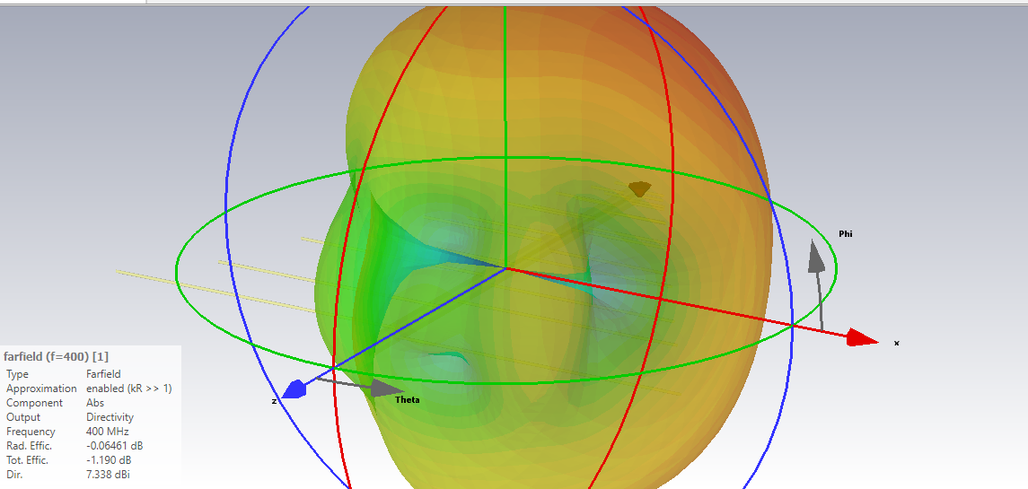
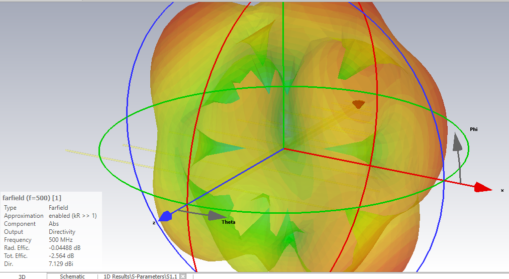
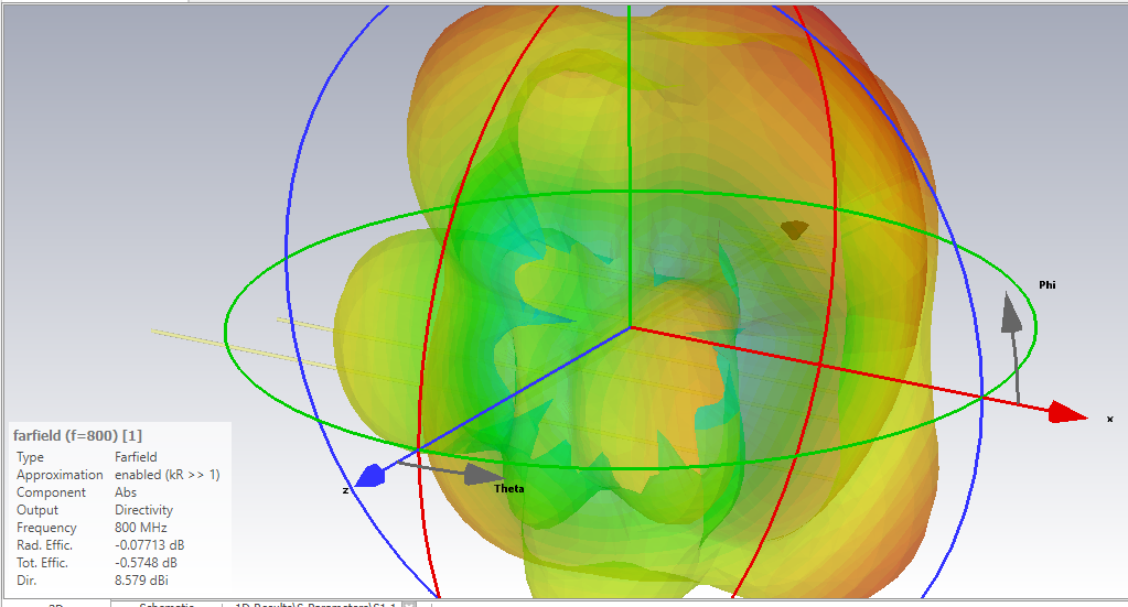
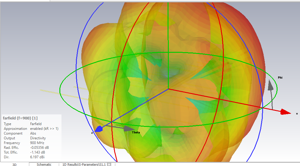
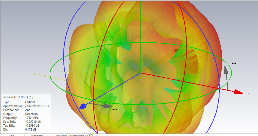
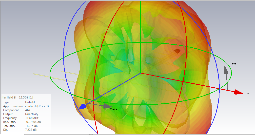
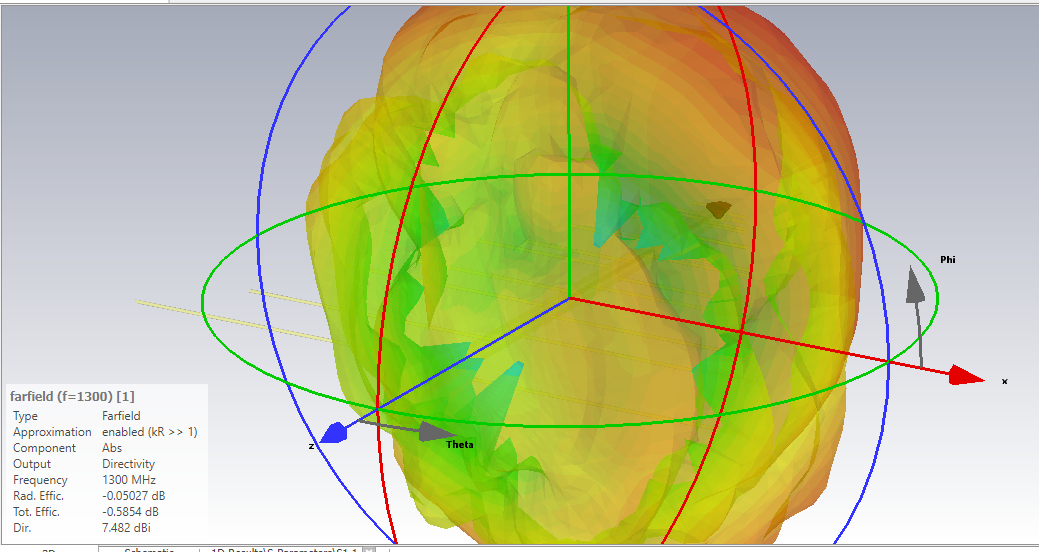
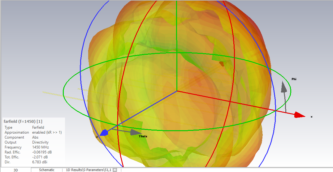
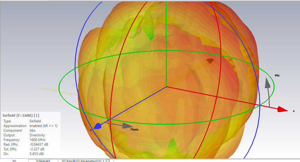
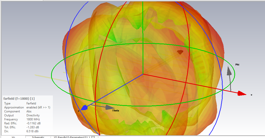
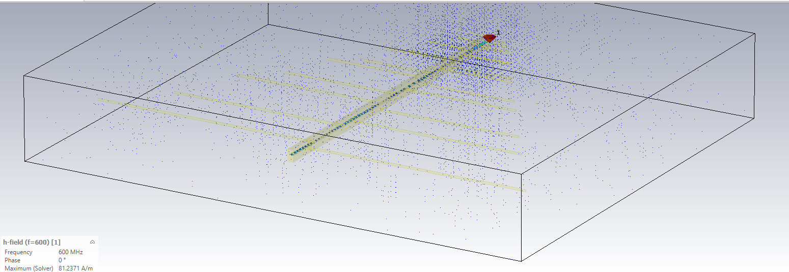
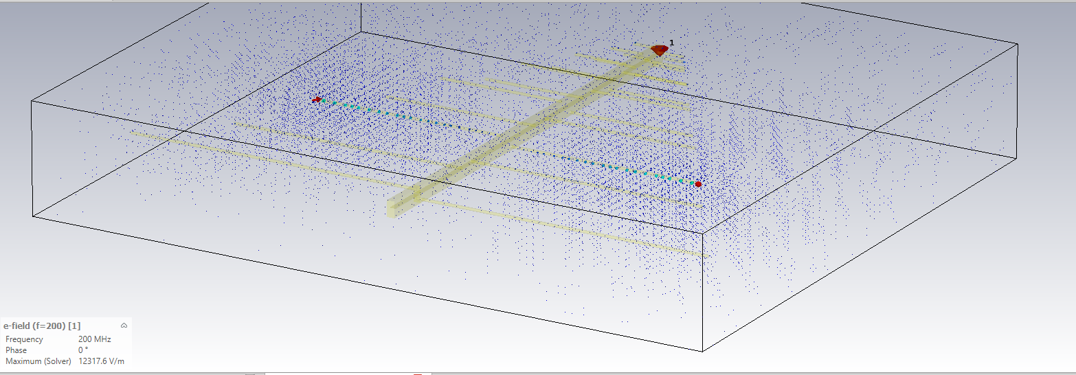
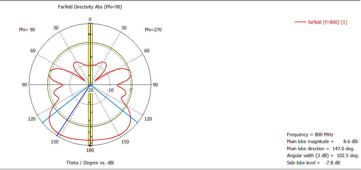
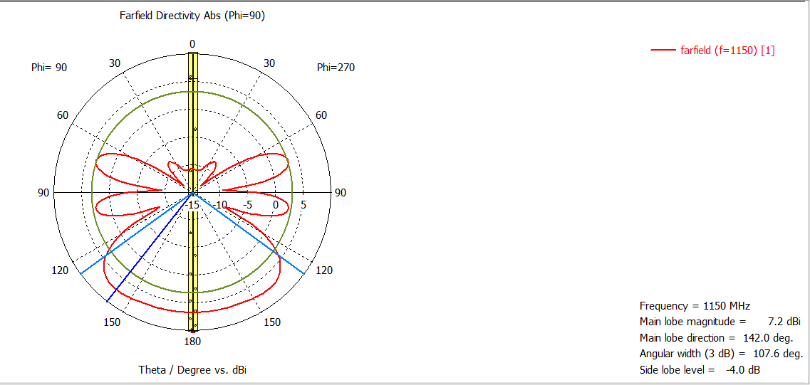
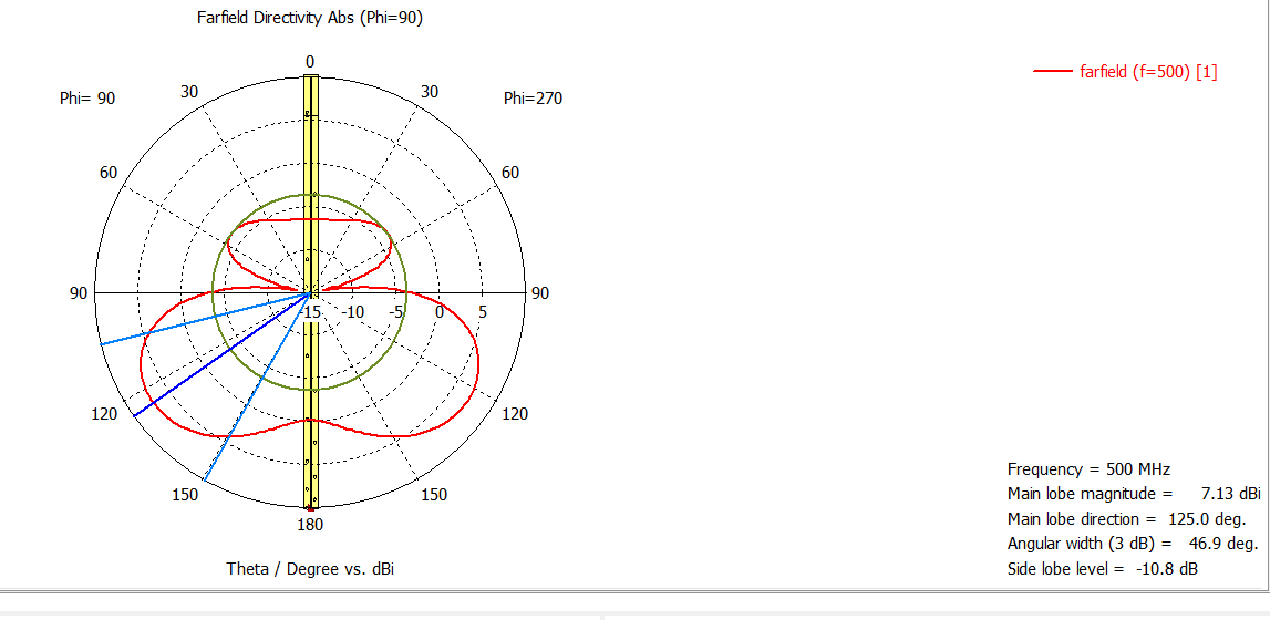
At any given frequency, only a small active region (typically about three elements) effectively radiates, and this active region shifts smoothly along the array as frequency changes. The antenna is usually fed from the shortest element, with the longest element acting as a reflector.
LPDA vs. Yagi–Uda Array
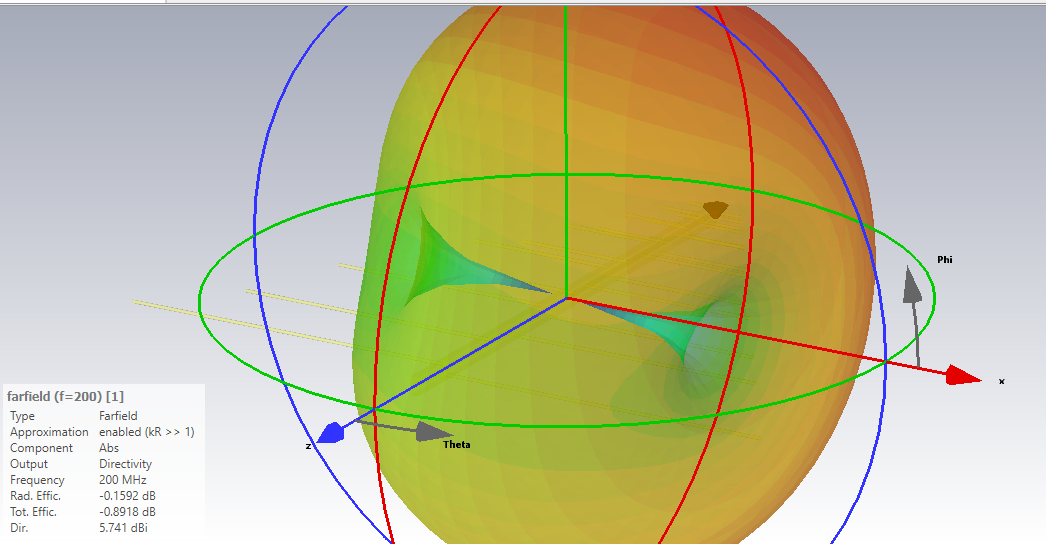
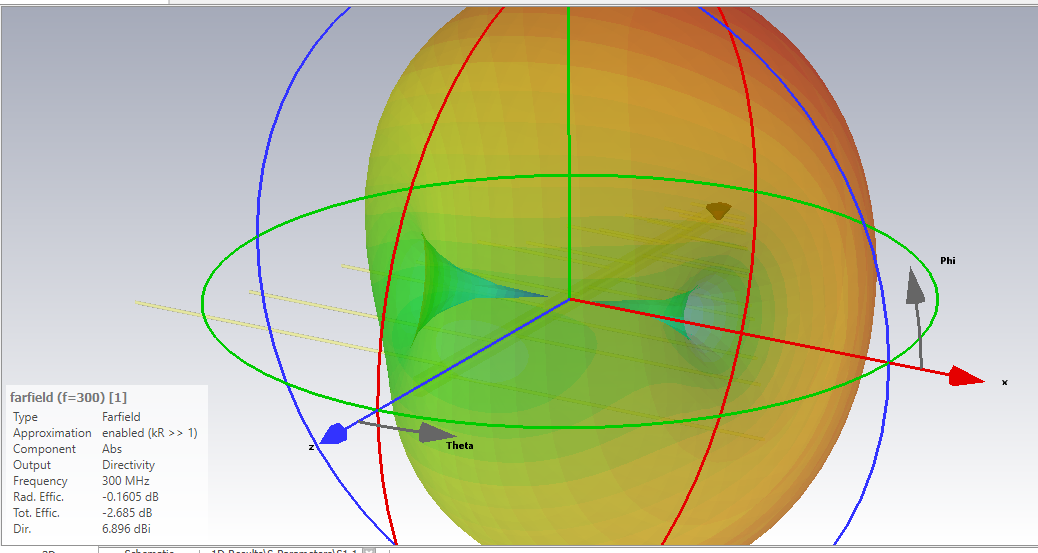
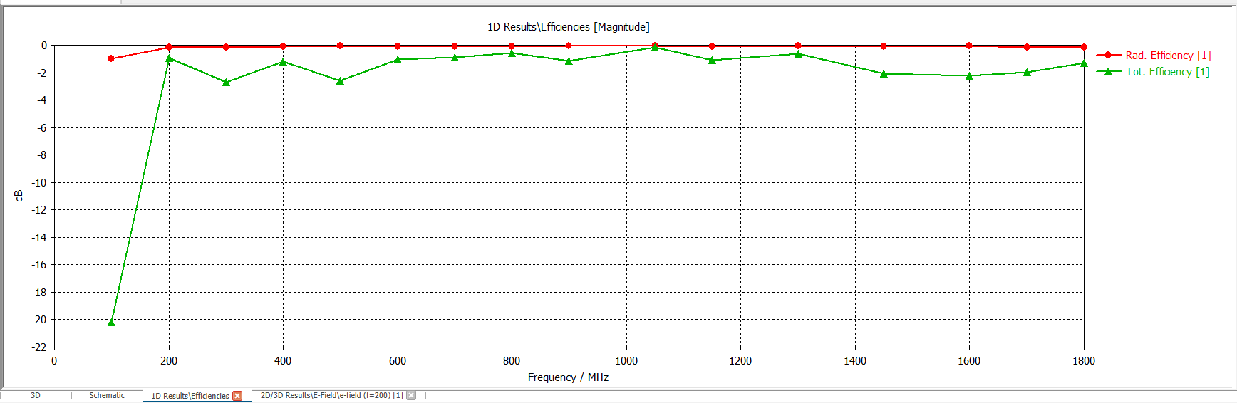
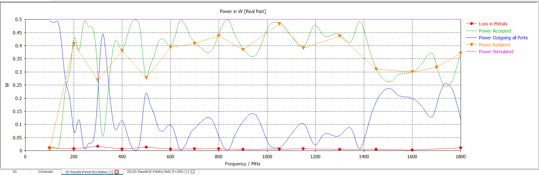
Yagi–Uda antennas provide high, narrowband gain at a specific frequency and are highly directional. In contrast, LPDAs offer moderate gain (≈5–15 dBi) over a wide frequency range with broader radiation patterns and lower directivity. LPDAs typically operate from 30–4200 MHz, while Yagi antennas operate from 30–3000 MHz. Yagi antennas focus energy into a narrow beam, whereas LPDAs provide wider coverage due to varying element lengths and spacing.
Advantages